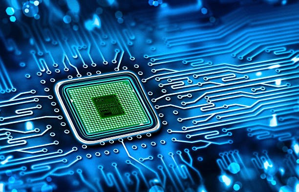
As semiconductor devices continue to scale in speed, density, and complexity, chip-level testing has become essential for ensuring product quality, yield, and reliability. Chip Test PCBs act as the interface between the chip under test and automated test equipment (ATE), providing precise signal routing, controlled impedance, and high-density connections for accurate semiconductor validation.
High-quality chip test PCBs enable engineers to perform functional testing, parametric measurements, and burn-in validation efficiently, ensuring that only fully verified ICs move into production.
What Is a Chip Test PCB?
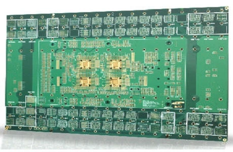
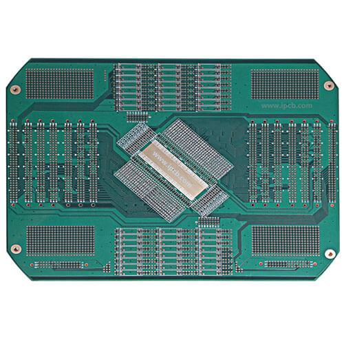
A Chip Test PCB is a specialized printed circuit board designed to connect directly to semiconductor chips via test sockets, probe cards, or load boards. Its primary functions include:
-
Routing high-density signals from the chip pads to the test equipment
-
Maintaining controlled impedance for high-speed and RF signals
-
Supporting high pin count connections and fine-pitch interfaces
-
Providing mechanical stability for accurate probe alignment and repeated test cycles
These PCBs are designed for accuracy, repeatability, and reliability in demanding semiconductor testing environments.
Key Features of Chip Test PCBs
-
High-Density Routing
Supports ICs with thousands of pins, fine-pitch BGA packages, or advanced wafer-level designs. -
Controlled Impedance
Essential for high-speed digital, RF, and mixed-signal testing to prevent signal reflection and loss. -
Multilayer Stackup
Enables separate power and ground planes, reduces crosstalk, and ensures signal integrity. -
Mechanical Precision
Accurate alignment for probe cards and sockets reduces pad damage and improves test repeatability. -
Thermal and Electrical Reliability
Withstands burn-in testing, high-current measurements, and repeated mechanical stress.
Materials and Stackup Considerations
Selecting the right materials and stackup is critical for chip test PCB performance:
-
High-Tg FR-4 – Standard choice for low-to-medium frequency chip testing
-
Low-Loss Laminates – Required for high-speed and RF IC testing
-
Hybrid Stackups – Combine standard FR-4 with low-loss cores for optimized performance
-
Thermally Stable Materials – Maintain dimensional stability during extended burn-in testing
Proper material and stackup design ensures signal integrity, mechanical reliability, and long-term PCB performance.
Applications of Chip Test PCBs
Chip test PCBs are widely used in:
-
Functional and parametric testing of ICs
-
Wafer-level burn-in and reliability testing
-
Load boards and probe card interfaces in ATE systems
-
High-speed digital, RF, and mixed-signal semiconductor validation
-
Prototype and small-batch chip testing before mass production
These applications benefit from the accuracy, repeatability, and high-density routing provided by chip test PCBs.
Choosing a Chip Test PCB Manufacturer
When selecting a chip test PCB supplier, consider:
-
Expertise in high pin count, high-speed, and multilayer PCB designs
-
Capability for controlled impedance, low-loss materials, and precise routing
-
Support for prototype, small batch, and volume production
-
Strong quality control, electrical verification, and mechanical testing
-
Responsive engineering support for design iteration and problem-solving
A professional partner ensures repeatable test results, high reliability, and fast turnaround.
Conclusion
Chip Test PCBs are essential for modern semiconductor testing, providing high-density routing, controlled impedance, and mechanical precision. They enable accurate IC validation, reliable burn-in testing, and seamless integration with ATE systems.
Partnering with an experienced chip test PCB manufacturer ensures high-quality performance, reduced testing errors, and faster time-to-market for your semiconductor products.
