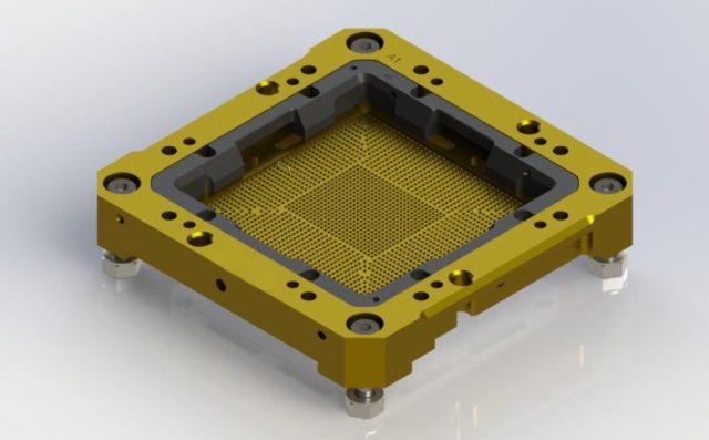
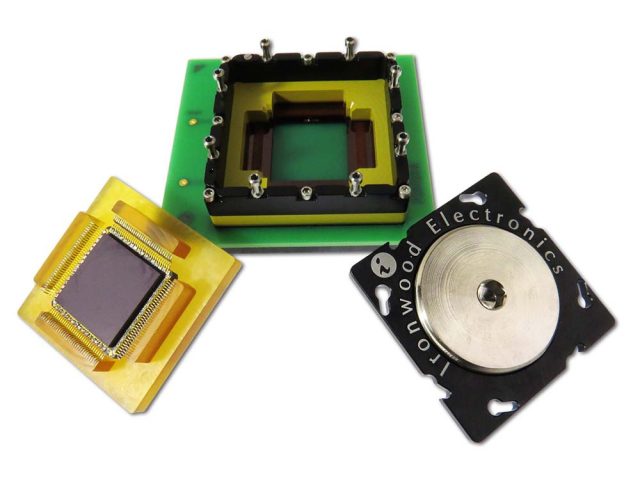
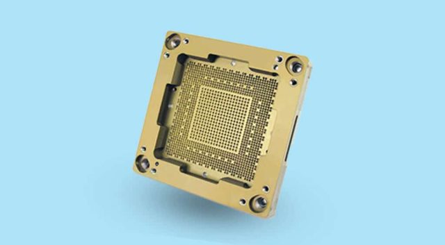
A Test Socket PCB for IC is a specialized semiconductor test PCB designed to interface ICs with Automated Test Equipment (ATE) through high-precision test sockets. These PCBs provide reliable electrical connectivity, controlled impedance, and mechanical stability, enabling accurate functional and performance testing of ICs before packaging or deployment.
As semiconductor devices evolve with higher pin counts, finer pitches, and higher-speed operation, test socket PCBs must meet strict requirements for signal integrity, mechanical precision, and thermal stability.
Key Design Requirements of Test Socket PCBs for ICs
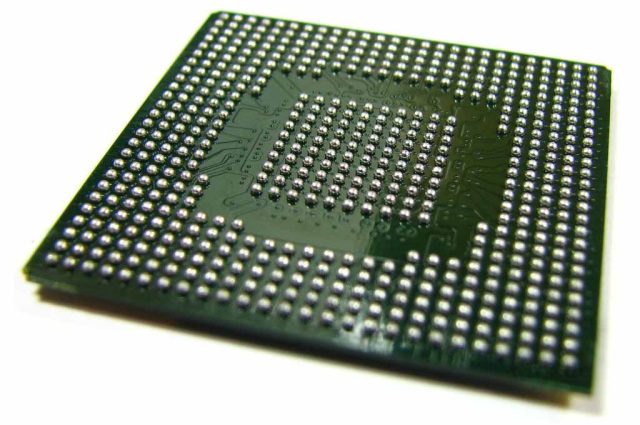
1. High Pin Count and Dense Routing
Modern ICs often have hundreds or thousands of pins. Test socket PCBs must use HDI technology, microvias, and fine-line routing to manage dense fanout while maintaining high signal fidelity.
2. Controlled Impedance and Signal Integrity
To ensure accurate high-speed IC testing, PCBs require precise controlled impedance, matched trace lengths, and low crosstalk, maintaining signal quality across all test channels.
3. Mechanical Accuracy and Reliability
The PCB must maintain pad alignment, flatness, and dimensional stability to guarantee consistent contact between the IC and the test socket during repeated testing cycles.
4. Power Distribution and Noise Control
Optimized power planes, low-impedance ground, and decoupling strategies ensure stable voltage supply to the IC, minimizing noise and fluctuations during high-speed functional testing.
5. Thermal Stability and Material Selection
Test socket PCBs must endure thermal stress from extended testing. Using high-Tg, low-loss laminates ensures electrical and mechanical performance remain stable under elevated temperatures.
Applications of Test Socket PCBs
Test Socket PCBs for ICs are widely applied in:
-
Logic IC and processor testing
-
Memory IC and DRAM validation
-
Mixed-signal and RF IC functional testing
-
Automotive semiconductor qualification
-
High-speed and high-reliability IC evaluation
These applications demand precise electrical contact, reliable connectivity, and repeatable measurement results.
Manufacturing Requirements for Test Socket PCBs
Producing reliable test socket PCBs for ICs requires:
-
Multilayer and HDI PCB fabrication
-
Microvia and blind/buried via technology
-
Controlled impedance verification and fine-line routing
-
High pin count and tight tolerance processing
-
Prototype, small batch, and volume production capabilities
Precision manufacturing ensures consistent electrical performance, high signal integrity, and long-term durability.
Why Test Socket PCB Quality Matters
Low-quality test socket PCBs can lead to:
-
Unstable IC contact and signal degradation
-
Inaccurate test results and false failures
-
Increased equipment downtime and maintenance costs
-
Reduced IC yield and higher production expenses
High-quality Test Socket PCBs guarantee reliable IC testing, accurate measurements, and consistent performance in demanding ATE environments.
Conclusion
The Test Socket PCB for IC is an essential component in automated IC testing, providing precise electrical routing, controlled impedance, and robust mechanical design. Advanced HDI layouts, high pin count routing, and premium materials ensure these PCBs deliver accurate, repeatable, and reliable testing for modern semiconductor devices.
Partnering with an experienced test socket PCB manufacturer ensures high test accuracy, improved yield, and long-term reliability across high-speed, mixed-signal, and high-density IC applications.
