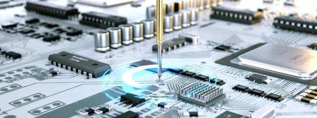
In semiconductor testing, time-to-market and development efficiency are critical. Small batch ATE PCBs provide a flexible solution for engineers who need rapid prototyping, functional validation, and low-volume production without compromising performance or reliability.
These PCBs are designed to handle high-density connections, controlled impedance, and stable signal integrity, making them essential for modern automated test equipment (ATE) environments.
What Is a Small Batch ATE PCB?
A small batch ATE PCB refers to a limited-quantity printed circuit board produced for semiconductor testing applications. These PCBs allow engineers to:
-
Validate IC designs and test fixture compatibility
-
Verify signal integrity in high-speed circuits
-
Iterate on designs rapidly before mass production
Small batch production ensures faster feedback and lower development risk compared to large-volume orders.
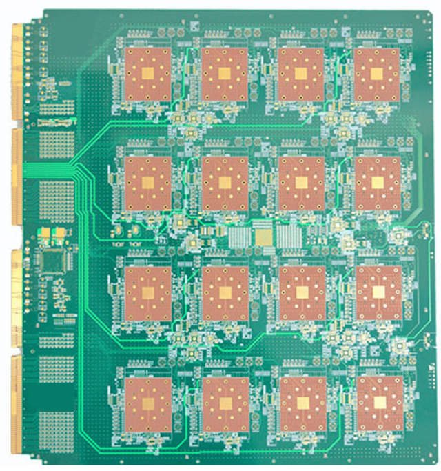
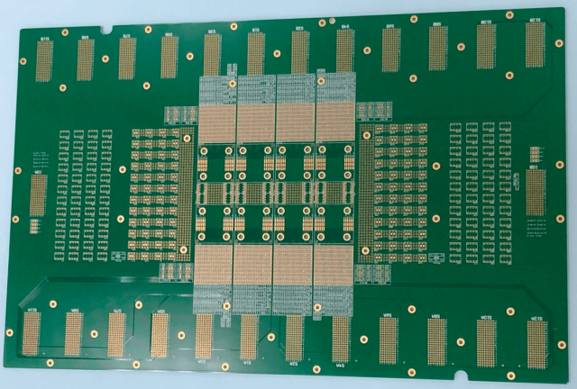
Key Features of Small Batch ATE PCBs
To meet the demands of semiconductor testing, small batch ATE PCBs include:
-
High Pin Count Support – Efficiently break out complex ICs for test connections.
-
Controlled Impedance Routing – Maintain signal integrity for high-speed or RF devices.
-
Multilayer Stackups – Accommodate dense routing and multiple power/ground planes.
-
Rapid Turnaround – Short lead times enable faster prototyping and engineering iteration.
-
Reliable Assembly – Durable solder joints and accurate component placement for repeated test cycles.
These features make small batch ATE PCBs ideal for prototype validation and pilot testing.
Material and Stackup Considerations
Small batch ATE PCB performance depends on careful material and stackup selection:
-
High-Tg FR-4 – Suitable for general test boards and moderate-speed applications.
-
Low-Loss Laminates – Essential for high-frequency or high-speed circuits.
-
Hybrid Stackups – Balance cost and electrical performance for small volume production.
Proper stackup design ensures controlled impedance, minimal signal loss, and mechanical reliability.
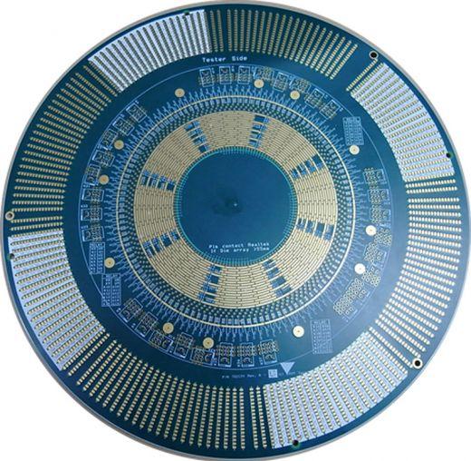
Applications of Small Batch ATE PCBs
Small batch ATE PCBs are commonly used in:
-
Semiconductor IC validation and characterization
-
Load boards and interface boards for ATE systems
-
Wafer-level testing and probe card development
-
High-speed digital and mixed-signal testing
They are particularly useful during early development, pilot runs, and functional verification before scaling to volume production.
Choosing a Small Batch ATE PCB Supplier
When selecting a small batch ATE PCB manufacturer, consider:
-
Experience with high pin count, high-speed, and multilayer test PCB designs
-
Capability for rapid prototyping and low-volume assembly
-
Comprehensive electrical testing and quality assurance procedures
-
Strong engineering support for design optimization and iteration
A professional partner ensures fast delivery without sacrificing PCB performance or reliability.
Conclusion
Small batch ATE PCBs provide a strategic advantage for semiconductor test engineering, enabling rapid prototyping, functional validation, and low-volume production. By combining controlled impedance, high-density routing, and fast delivery, small batch ATE PCBs help accelerate product development, reduce risk, and improve testing efficiency.
