Single Layer PCBs: A Comprehensive and Technical Guide
Introduction
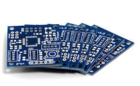
Single-layer printed circuit boards (PCBs)—often referred to as single-sided or 1-layer PCBs—represent the most fundamental yet enduring form of PCB technology. Despite the fast-growing adoption of multilayer, HDI, and advanced substrate solutions, single-layer boards continue to dominate large segments of consumer electronics, industrial instrumentation, IoT nodes, simple power supplies, and cost-sensitive applications.
Their appeal is clear:
✔ low material cost
✔ straightforward manufacturing
✔ fast prototyping
✔ stable electrical performance for simple circuits
This guide delivers a systematic, professional-level overview of single-layer PCBs—from structural fundamentals and design methodologies to manufacturing processes, cost drivers, and modern applications.
What Is a Single Layer PCB?
A single-layer PCB features one copper layer laminated on an insulating substrate. All components and routing occur on this single conductive side, making the structure simple yet highly reliable for low to moderate circuit complexity.
Core Structure of a Single-Layer PCB
Layer |
Function |
|---|---|
| Substrate (Core) | Mechanical support + insulation (typically FR-4, CEM-1, phenolic) |
| Copper Layer | Etched into conductive traces; thickness often 1 oz / 2 oz depending on current requirement |
| Solder Mask | Protects traces from oxidation and solder bridging; most often green |
| Silkscreen | Component labels, polarity markers, and assembly information |
Advantages
-
Extremely cost-effective
-
Fast turnaround and high manufacturability
-
 Ideal for high-volume production
 -
Lower risk of signal integrity issues due to simple topology
-
Good thermal performance for low-power circuits
Limitations
-
Limited routing area
-
Not suitable for complex or high-density systems
-
Limited EMC optimization options
-
Restricted to low- to moderate-current and low-speed applications
Design Considerations for Single Layer PCBs
Although structurally simple, single-layer PCB design still requires rigorous engineering to ensure signal quality, manufacturability, and reliability.
1. Schematic Engineering
A stable design starts with:
-
Correct component selection
-
Clear signal flow planning
-
Proper power distribution
-
Adequate decoupling strategy
Ground integrity is especially important since only one routing layer is available. Large copper pours are recommended to reduce noise and improve return-path consistency.
2. Component Placement
Effective placement ensures:
-
Shorter trace lengths
-
Reduced crosstalk and EMI
-
Better thermal distribution
-
Easier assembly and maintenance
Functionally related components should be grouped logically to minimize routing congestion.
3. Routing Strategy
Key rules include:
-
Use proper trace width (based on current)
-
Maintain sufficient clearance for manufacturability
-
Prefer 45° routing instead of right angles
-
Avoid long or unnecessary loops
-
Maintain strong ground continuity
4. EMC and Noise Control
Since single-layer boards lack ground planes:
-
Include local decoupling capacitors
-
Use copper pours as pseudo-ground planes
-
Separate noisy and sensitive circuits
-
Avoid parallel long traces carrying high-frequency signals
5. DFM (Design for Manufacturability)
Adhere to fabrication constraints:
-
Minimum trace width/spacing
-
Drill-to-copper clearance
-
Standard hole sizes
-
Pad-to-trace transition integrity
Designing with manufacturability in mind reduces cost and increases yield.
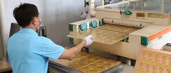
Single Layer PCB Manufacturing Process
Although simpler than multilayer fabrication, single-layer PCB production still requires precise process control.
Manufacturing Workflow
-
Base Material Preparation
Cutting and cleaning FR-4 or other substrates. -
Lamination & Photoresist Coating
Preparing copper-clad panels for imaging. -
Exposure & Development
UV imaging transfers the circuit pattern onto the copper. -
Etching
Removes unwanted copper, leaving only the designed traces. -
Drilling
Creates mounting holes and through-holes for TH components. -
Solder Mask Application
Insulates and protects the copper surfaces. -
Silkscreen Printing
Adds component identifiers and assembly text. -
Surface Finish Application
Common surface treatments:-
HASL (Hot Air Solder Leveling) — economical
-
ENIG — flat, oxidation-resistant
-
OSP — eco-friendly, low-cost
-
-
Testing & Inspection
-
AOI for trace integrity
-
Electrical testing for shorts/opens
-
Cost Structure of Single Layer PCBs
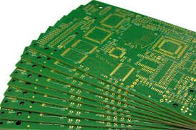
Single-layer PCBs are the lowest-cost PCB category, typically ranging from $0.10 to $5 per unit depending on size, material, finish, and quantity.
Why Single Layer PCBs Are Inexpensive
-
Minimal material usage
Only one copper layer and no lamination cycles. -
Simplified fabrication
No multi-stage alignment, multilayer lamination, or buried/blind via processes. -
Higher manufacturing yield
Fewer failure points and simpler inspection.
These factors make single-layer PCBs ideal for cost-driven applications.
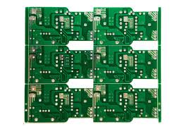
Typical Applications of Single Layer PCBs
Single-layer PCBs remain vital in industries where simplicity, cost-efficiency, and reliability matter most.
1. Consumer Electronics
-
Remote controls
-
LED lighting modules
-
Household appliances
-
Audio systems
2. Industrial Control
-
Relay modules
-
Sensor interfaces
-
Simple automation controllers
3. Power Electronics
-
AC–DC adapters
-
Charger circuits
-
Small power supplies
4. Medical & Instrumentation
-
Portable diagnostic devices
-
Basic monitoring modules
5. IoT & Embedded Systems
Especially for ultra-low-cost IoT nodes where minimal circuitry is required.
Future Trends of Single Layer PCBs
Even as electronics become more complex, single-layer PCBs continue to evolve.
Key Development Directions
-
Eco-friendly substrate materials (halogen-free, bio-resin-based)
-
Finer etching capability enabling higher routing density
-
Integration with flexible PCB technologies
-
Large-scale adoption in IoT and smart home devices
-
Improved automation in fabrication for faster turnaround
The need for low-cost, high-reliability PCBs ensures that single-layer designs will remain an essential foundation of modern electronics.
Conclusion
Single-layer PCBs offer a compelling balance of simplicity, reliability, short lead times, and ultra-low cost. They are indispensable in consumer electronics, industrial controllers, IoT devices, and fundamental power circuits. As manufacturing innovation continues—along with growing demand for low-cost, compact electronics—single-layer PCBs remain an important and irreplaceable technology.
