1. Introduction
In advanced RF and microwave test systems, where signal accuracy defines measurement integrity, the substrate material directly determines consistency.
The RF-35 PCB—a low-loss laminate with optimized dielectric uniformity—has become a preferred platform for network analyzers, calibration modules, and power sensors operating between 20 GHz to 50 GHz.
KKPCB’s engineering framework addresses key parameters including phase stability, insertion-loss linearity, and impedance control, which are critical to achieving long-term measurement repeatability.
2. Core Engineering Challenges
| Challenge | Impact on Measurement | Engineering Concern |
|---|---|---|
| Dielectric Variation | Phase shift, calibration drift | Tight Dk tolerance (±0.05) required |
| Loss Tangent | Reduced dynamic range | Must stay below 0.0018 @10 GHz |
| Thermal Expansion | Connector misalignment | CTE balance across multilayers |
| Impedance Control | Return loss, mismatch | ±5% trace tolerance critical |
| Mechanical Stability | Repeatability under thermal cycles | Requires low-z-axis expansion |
RF-35 PCB boards face particular difficulty in balancing signal integrity and thermal dimensional stability, especially in VNA and spectrum analyzer test fixtures subjected to repeated thermal cycling.
3. KKPCB Engineering Solution Framework
KKPCB’s engineering approach integrates material uniformity, hybrid stackup optimization, and precision etching to sustain consistent measurement response:
-
Hybrid Stackup Integration:
RF-35 PCB is combined with FR-4 or PTFE support cores to achieve mechanical rigidity while preserving dielectric consistency. -
Advanced Impedance Control:
Microstrip and grounded coplanar waveguide (GCPW) structures are simulated in HFSS with ±0.03 mm etching tolerance. -
Phase Stability Assurance:
Phase shift variation remains below 1.2°/GHz/inch across the 10–40 GHz range through dielectric pre-conditioning and matched copper surface roughness. -
Surface Finish Optimization:
Electroless Nickel Immersion Gold (ENIG) plating is limited to < 4 µin to prevent additional loss at mmWave frequencies.
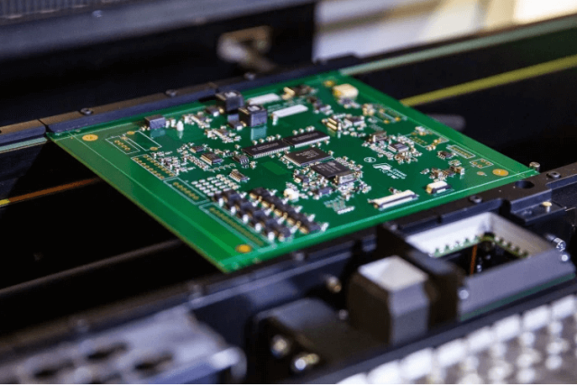
RF-35 PCB
4. Case Study — Precision Calibration Module (40 GHz)
| Parameter | Test Result | Standard Deviation |
|---|---|---|
| Insertion Loss (20 GHz) | 0.28 dB | ±0.03 dB |
| Phase Stability (30 GHz) | ±1.5° | ±0.2° |
| Return Loss | –27 dB | — |
| Temperature Drift (–40 °C ~ +125 °C) | < 0.04 dB | — |
A calibration module built on KKPCB RF-35 PCB substrate demonstrated superior signal-to-noise uniformity and reduced phase drift, achieving < 1 dB amplitude deviation even after 1000-hour thermal reliability testing.
5. Reliability Validation
KKPCB performs multiple qualification stages:
-
Thermal Shock (–55 °C to +150 °C, 1000 cycles) — No layer delamination.
-
RF Power Endurance (10 W continuous, 40 GHz) — Stable insertion loss.
-
Humidity Exposure (85 °C / 85% RH for 500 h) — < 2% Dk shift.
-
Mechanical Bending Test (IPC-TM-650) — No microcrack formation under 2 mm flex.
6. Engineering Takeaway
For precision RF test and measurement systems, RF-35 PCB substrates deliver a highly stable electrical platform that maintains phase linearity, impedance control, and calibration repeatability across extended temperature and frequency ranges.
Through KKPCB’s controlled hybrid stackup and dielectric pre-conditioning, the design achieves both signal integrity and long-term measurement reliability, critical to modern mmWave instrumentation.
