What Is a a SiC PCB?
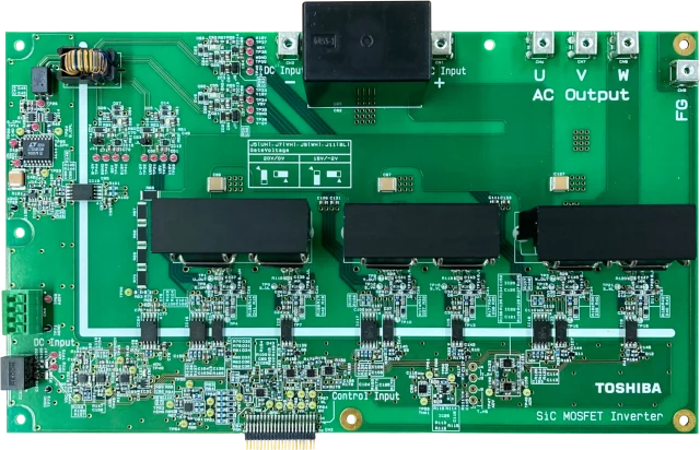
A SiC PCB is a printed circuit board designed to support silicon carbide (SiC) power semiconductor devices used in high-efficiency power electronics. Silicon carbide technology enables electronic systems to operate at higher voltages, higher temperatures, and higher switching frequencies compared to traditional silicon-based devices.
PCBs designed for SiC devices must meet strict requirements related to thermal management, high current capacity, and electrical reliability, since SiC components are commonly used in demanding power systems.
SiC PCBs are widely used in:
-
Electric vehicles (EV) and charging systems
-
Renewable energy inverters
-
Industrial motor drives
-
High-efficiency power converters
-
Aerospace power electronics
These applications require PCBs capable of handling high power density and stable electrical performance.
Characteristics of SiC Power Electronics
Silicon carbide devices offer several advantages over traditional semiconductor technologies. When integrated into PCB systems, they enable improved performance and energy efficiency.
Key characteristics include:
-
High voltage capability
-
High switching frequency
-
Low power loss
-
High thermal tolerance
-
Compact system design
Because SiC devices can switch faster and operate at higher temperatures, PCB design must ensure excellent heat dissipation and stable electrical pathways.
Thermal Management in SiC PCB Design
One of the most critical aspects of SiC PCB design is thermal management. High-power SiC devices generate significant heat during operation.
Effective thermal strategies include:
-
Thick copper layers for heat spreading
-
Thermal vias beneath power components
-
Metal core PCB structures
-
Direct bonding copper (DBC) substrates
These design methods help maintain safe operating temperatures and improve system reliability and lifespan.
High Current and Power Handling
SiC power systems often involve high current flows and high voltage switching, which requires PCB structures capable of supporting large power loads.
Design considerations include:
-
Wide copper traces for current carrying capacity
-
Heavy copper PCB structures
-
Optimized power plane layouts
-
Reinforced solder pads for power components
These features allow SiC PCBs to handle high power densities without performance degradation.
High-Speed Switching and Signal Integrity
SiC devices switch much faster than traditional silicon power components. While this improves efficiency, it also introduces challenges such as electromagnetic interference (EMI) and signal noise.
PCB designers address these challenges by implementing:
-
Short switching loop paths
-
Proper grounding structures
-
Controlled impedance signal routing
-
EMI reduction techniques
These practices ensure stable operation even in high-frequency power electronics environments.
Applications of SiC PCB
SiC PCBs are increasingly important in next-generation power electronics systems, including:
-
Electric vehicle traction inverters
-
Fast EV charging stations
-
Solar and wind power inverters
-
Industrial automation equipment
-
Aerospace power systems
In these applications, SiC technology enables higher efficiency, smaller system size, and improved energy conversion performance.
Conclusion
A SiC PCB plays a critical role in supporting silicon carbide power devices used in modern high-efficiency power electronics. By focusing on thermal management, high current handling, and optimized power layouts, these PCBs enable reliable operation in demanding applications.
As industries continue to adopt SiC technology for improved energy efficiency, advanced PCB solutions will remain essential for supporting next-generation power electronic systems.
