Rapid electronics development has entered an era where design cycles are measured not in months but in weeks. From IoT edge devices to next-generation communication modules and automotive sensing platforms, engineers must iterate faster while maintaining electrical performance, manufacturability, and long-term reliability. PCB prototypes sit at the heart of this acceleration. When engineered correctly, they collapse validation loops, reduce redesign risks, and provide accurate insight into a product’s real-world behaviour.
At KKPCB, PCB prototyping is treated as an engineering discipline rather than a procurement step. The goal is simple: minimize development friction while ensuring every prototype reflects mass-production quality and reliability.
1. Engineering for Speed: From Concept to Functional Boards
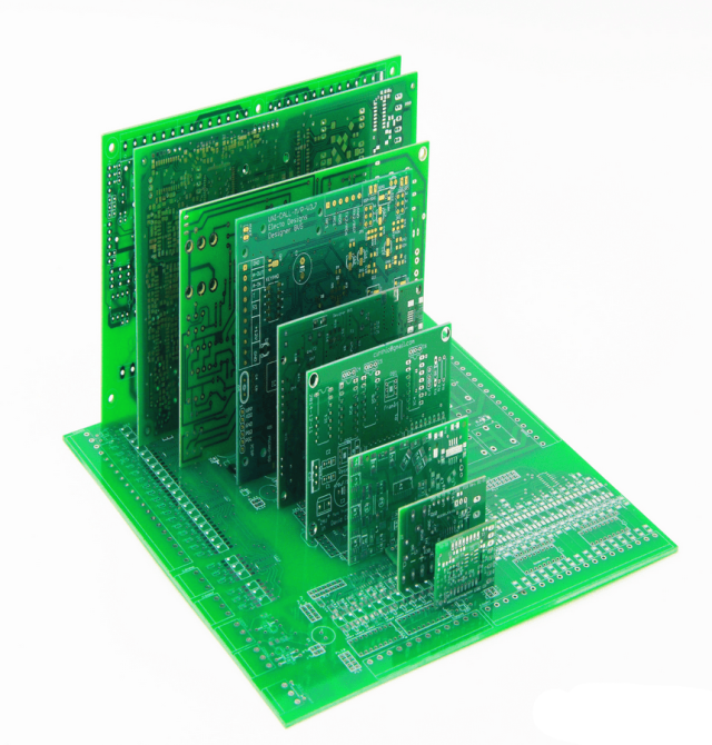
R&D teams often face delays not because of design mistakes, but because prototypes fail to represent actual production conditions. To solve this, the prototype workflow focuses on production-grade stackups, repeatable impedance performance, and predictable material behaviour.
Key engineering areas include:
• True-to-production stackups for multilayer and HDI boards
• Controlled impedance with ±5% trace accuracy for RF and high-speed interfaces
• Rapid DFM/DFT review to eliminate unnecessary redesign cycles
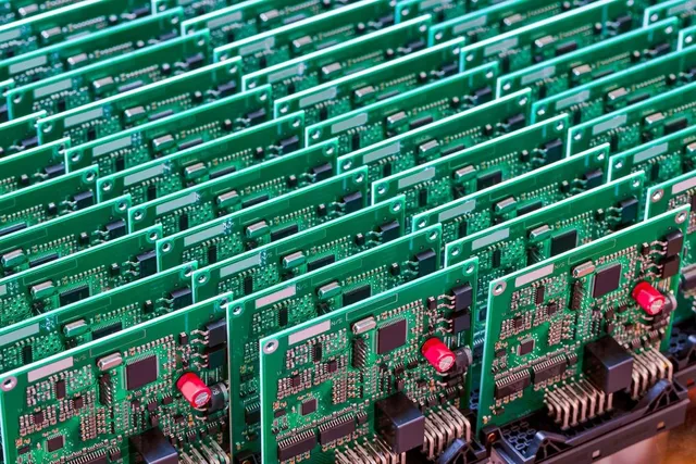
• Flexible build options: 2–20L in fast-turn, 10–36L for advanced R&D
This ensures every prototype behaves like a future mass-production sample, so each iteration brings meaningful progress rather than accidental noise.
2. Cost-Optimized Architecture Without Compromising Reliability
Cost-driven prototyping doesn’t mean cutting corners; it means making smart engineering choices.
Typical optimizations:
• Selecting the right laminate tier (FR-4 → Mid-Loss → Low-Loss) depending on signal speed
• Matching copper weights and via structures to early-stage electrical requirements
• Using mixed dielectric combinations for RF, power, and digital domains
• Implementing stackups that are simpler to build but still aligned with performance goals
These optimizations lower prototype expenses while preserving long-term electrical and mechanical stability, especially for teams running multiple iterations.
3. Reliability Metrics Baked Into Early Prototypes
Every prototype carries early reliability data that guides later decisions.
Key parameters embedded into prototype builds include:
• Thermal stability and Tg alignment for high-power modules
• Via reliability through microvia stacking rules & aspect-ratio control
• CAF prevention strategies to secure long-term insulation performance
• Solder-joint durability validated through reflow profile matching
By incorporating these metrics early, engineers avoid reliability regressions during scale-up.
4. Accelerating Multi-Disciplinary R&D Workflows
Modern electronics are no longer single-domain. A prototype must support:
• RF signal chains
• High-speed digital buses
• Power management
• Sensor integration
• EMI/EMC compliance pathways
KKPCB’s prototype workflows integrate early simulations (SI/PI guidance), controlled dielectric selection, and RF-sensitive routing strategies to reduce redesign loops across domains.
This shortens R&D timelines by providing engineers with boards that perform correctly the first time, even under mixed-signal stress.
5. Manufacturing Transparency That Reduces Guesswork
Clear communication reduces delays more effectively than any express service.
By providing early disclosure of:
• stackup maps
• plating thickness
• impedance tables
• drill/via charts
• copper distribution feedback
engineers can correct oversights before they become failures. This makes the prototype-to-production transition far smoother and avoids repeating the same engineering mistake across multiple cycles.
6. Supporting Rapid Development Models: Agile, Parallel, and Modular R&D
Modern R&D teams often run:
• parallel prototype builds
• modular sub-board verification
• phased functional trials
A prototype service must support this through consistent quality, stable electrical metrics, and flexible delivery windows. When each batch performs predictably, teams can safely run simultaneous experiments without unexpected electrical drift or fabrication deviation.
Conclusion
Shortening R&D cycles isn’t about working faster—it’s about removing delays, uncertainties, and engineering noise. Cost-optimized, high-reliability PCB prototypes provide the strongest leverage in this process, enabling rapid learning loops, stable electrical validation, and smoother production handoff.
When prototypes behave like production hardware, every iteration becomes a confident step toward market-ready electronics. This is where efficient engineering and well-structured PCB architecture turn development speed into a competitive advantage.
