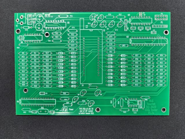
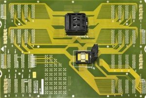
A Semiconductor Load Board PCB is a critical ATE (Automated Test Equipment) PCB used to interface between test equipment and semiconductor devices during electrical testing. These boards provide a reliable platform for signal routing, power delivery, and measurement of ICs, ensuring accurate evaluation of device performance before packaging or deployment.
With modern ICs moving toward higher pin counts, mixed-signal integration, and high-speed operation, load board PCBs must deliver high signal integrity, precise impedance control, and robust mechanical reliability.
Key Design Features of Semiconductor Load Board PCBs
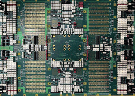
1. High Pin Count and Dense Interconnects
Load boards often accommodate ICs with hundreds or thousands of pins, requiring HDI PCB technology, fine-line routing, and multilayer stackups for reliable electrical connections.
2. Controlled Impedance and Signal Integrity
Accurate testing demands precise impedance control, trace length matching, and minimized crosstalk to maintain signal integrity across all test channels.
3. Robust Power Distribution and Noise Reduction
Optimized power planes, decoupling, and low-impedance ground networks ensure stable power delivery to the IC under test, reducing noise and voltage fluctuation during testing cycles.
4. Mechanical Accuracy and Durability
Load boards must maintain flatness, dimensional precision, and pad alignment for consistent and reliable contact with test sockets or probe cards, even after repeated test cycles.
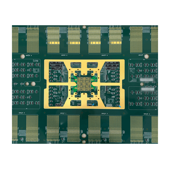
5. Thermal and Material Considerations
High-Tg, low-loss materials and robust multilayer construction allow reliable performance under thermal stress and high-power operation, critical for prolonged ATE testing.
Applications of Semiconductor Load Board PCBs
Semiconductor load boards are widely used in:
-
Logic and processor IC testing
-
Memory and storage device validation
-
RF, mixed-signal, and high-speed IC evaluation
-
Automotive and industrial semiconductor testing
-
High-reliability IC qualification for aerospace applications
These applications require precision, reliability, and repeatability from the load board PCB.
Manufacturing Requirements for Semiconductor Load Board PCBs
High-quality load boards require:
-
HDI and multilayer PCB fabrication
-
Fine-line etching and microvia technology
-
Controlled impedance verification
-
High pin count and tight tolerance processing
-
Prototype, small batch, and volume production capabilities
Advanced manufacturing ensures consistent electrical performance, long-term reliability, and high test accuracy.
Why Semiconductor Load Board PCB Quality Matters
Inferior load boards can result in:
-
Poor electrical contact and signal degradation
-
Inaccurate IC test results
-
Increased equipment downtime and maintenance
-
Reduced test yields and higher production costs
A high-quality Semiconductor Load Board PCB guarantees reliable IC testing, repeatable measurements, and optimal performance of automated test systems.
Conclusion
The Semiconductor Load Board PCB is a fundamental component in IC testing and ATE systems, providing precise signal routing, controlled impedance, and mechanical stability. By leveraging advanced HDI design, multilayer construction, and high-quality materials, load boards ensure reliable and repeatable testing for modern semiconductor devices.
Partnering with a professional load board PCB manufacturer ensures high measurement accuracy, improved yield, and consistent ATE performance for advanced IC applications.
