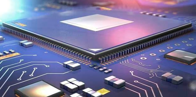
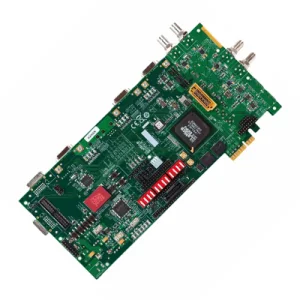
In modern semiconductor testing, Semiconductor Load Board PCBs are a critical component of Automated Test Equipment (ATE) systems. These PCBs serve as the essential interface between devices under test (DUTs) and testing instruments, ensuring high-speed signal integrity, accurate voltage delivery, and precise mechanical alignment throughout IC, memory, and RF chip testing.
As ICs and memory devices continue to evolve with higher pin counts, faster data rates, and more complex packages, designing and manufacturing high-quality load board PCBs has become increasingly challenging. A well-engineered Semiconductor Load Board PCB provides reliable electrical connections, controlled impedance, and mechanical precision, ensuring consistent, repeatable, and accurate test results across production and R&D environments.
Key Features of Semiconductor Load Board PCBs
-
High Pin Count and Dense Routing
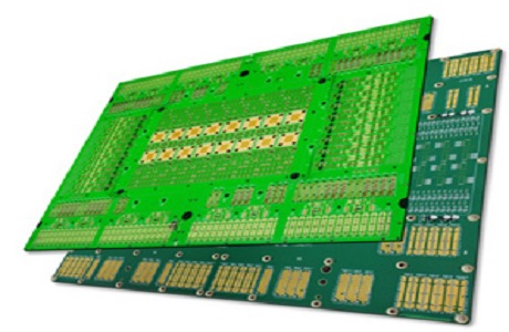
Advanced ICs and memory modules often require hundreds to thousands of connections. Load board PCBs are designed with fine-line and high-density HDI routing to accommodate these complex packages. -
Controlled Impedance for High-Speed Signals
Maintaining controlled impedance is critical for high-speed digital, RF, and microwave testing, minimizing crosstalk, signal reflection, and jitter. -
Stable Power Distribution and Low-Loss Signal Paths
Proper power plane design and low-loss laminates reduce voltage fluctuations and maintain signal fidelity during rigorous ATE testing. -
Mechanical Precision and Repeatability
High-quality load boards ensure accurate socket and probe alignment, maintaining consistent contact force across thousands of test cycles. -
Multilayer and Rigid-Flex PCB Options
Multilayer stackups and rigid-flex PCB technology allow complex routing and space-efficient designs, meeting the demands of advanced semiconductor testing.
Applications of Semiconductor Load Board PCBs
Semiconductor Load Board PCBs are widely used in:
-
IC Testing PCB for logic, analog, and mixed-signal devices
-
Memory Test PCB for DRAM, SRAM, Flash, and NAND modules
-
RF and Microwave IC Test PCB for high-frequency device validation
-
Wafer Test PCB and Probe Card Assembly integration
-
Automotive, IoT, and high-reliability semiconductor production testing
These applications require high-speed signal integrity, low-loss routing, and mechanical reliability, all of which are enabled by professional load board PCB design and manufacturing.
Material and Manufacturing Considerations
Choosing the right materials and fabrication techniques is critical for Semiconductor Load Board PCB performance:
-
High-Tg FR-4 for standard IC and memory test applications
-
Low-loss RF laminates for high-speed or RF/microwave testing
-
Hybrid stackups combining FR-4 with RF laminates for mixed-signal load boards
-
HDI and microvia technology for high-density and high-pin-count designs
-
Precision surface finishes for probe and socket reliability
Proper materials ensure signal integrity, dimensional stability, and long-term reliability even under repeated test cycles.
Why Choose a Professional Load Board PCB Manufacturer
Selecting a trusted load board PCB manufacturer is critical to maintain accuracy, repeatability, and reliability in semiconductor testing. Key capabilities include:
-
Expertise in high-pin-count, multilayer, and HDI PCB designs
-
Ability to deliver small-batch prototyping and high-volume production
-
Strong quality control, electrical testing, and engineering support
-
Proven experience with IC, memory, and RF test systems
A professional manufacturer ensures faster validation cycles, reduced test failures, and improved production yield, making them an indispensable partner for semiconductor companies.
Conclusion
Semiconductor Load Board PCBs are a vital component of modern ATE systems, enabling high-density routing, controlled impedance, low-loss signal transmission, and precise mechanical alignment. From ICs and memory devices to RF and microwave chips, high-quality load board PCBs ensure accurate, repeatable, and reliable semiconductor testing, helping manufacturers achieve higher yields, faster time-to-market, and more efficient test operations.
