RF PCB Design for 5G Devices: High-Frequency Architecture, Antenna Integration & Engineering Best Practices
Designing RF PCBs for 5G hardware is far more than simple high-speed layout—it requires a deep command of electromagnetic behavior, antenna engineering, high-frequency signal routing, impedance control, and noise isolation.
In next-generation wireless systems, the antenna is no longer a passive component—it directly defines link budget, range, spectral efficiency, and overall device performance.
This guide provides a comprehensive, engineer-oriented breakdown of 5G RF PCB design principles, antenna integration strategies, and practical layout considerations to help you build reliable, production-ready radio systems.
1. Key Principles of 5G RF PCB Engineering
High-frequency PCB success depends on four essential design pillars:
Antenna integrity & placement
Antenna performance degrades dramatically if placed near metal structures, noisy components, or inconsistent ground references.
Controlled impedance signal paths
5G frequencies (sub-6 GHz to mmWave) require extremely tight impedance tolerance to avoid reflections and insertion loss.
Low-noise RF layout
5G radios are extremely sensitive to power noise, switching harmonics, and digital coupling.
Material selection
Ceramic-filled PTFE, hydrocarbon laminates, and low-loss dielectrics are preferred over FR-4 for stable signal propagation.
2. Selecting Antennas for 5G & IoT PCB Designs
Modern PCB-integrated antennas typically operate from 400 MHz to 5.5 GHz, with mmWave extensions for advanced 5G NR bands.
Choosing the correct antenna requires balancing:
Essential Selection Criteria
-
Frequency band
-
Antenna size
-
Form factor
-
Radiation pattern
-
Gain requirements
-
Polarization
-
Ground plane constraints
-
Cost
5G Trend: High-Gain Miniature Antennas
5G and IoT devices increasingly rely on compact, multi-band antennas with higher gain to support dense connected environments and high throughput.
This drives heavy adoption of MIMO arrays—with 8×8 configurations becoming standard in many LTE-Advanced and 5G platforms.
3. PCB Antennas: Types & Design Considerations
PCB antennas are cost-efficient and easy to manufacture, though they require careful layout discipline.
3.1 PCB Antenna Categories
-
Inverted-F antenna (IFA)
-
Meandered inverted-F antenna (MIFA)
-
Inverted-L
-
Folded monopole
-
Meandered trace
-
Circular trace
The ground plane is the dominant factor influencing bandwidth, radiation efficiency, and field uniformity.
3.2 Dipole & Monopole Antennas
Dipole Antennas
Two linear conductive elements—less common in compact 5G devices.
Quarter-Wave Monopole Antennas
-
Most widely used in PCB designs
-
Fed single-ended
-
Ground plane acts as the mirror element
-
Suitable for both sub-6 GHz and mmWave bands (24–100 GHz)
3.3 Inverted-F Antennas (IFA)
A robust, compact antenna structure ideal for BLE, Wi-Fi, and mid-band 5G applications.
Advantages
-
Small size
-
Efficient radiation
-
Easy impedance matching
-
Direct PCB integration with no external components
Feed Line Optimization
Antenna feed width depends on PCB thickness (FR-4, Er 4.3):
Thickness (mil) |
Feed Width W (mil) |
|---|---|
| 60 | 65 |
| 50 | 59 |
| 40 | 52 |
| 30 | 44 |
| 20 | 33 |
3.4 Meandered-IFA (MIFA)
Designed where PCB area is extremely limited—ideal for wearables, mice, presenters, and compact BLE modules.
Antenna length depends on PCB thickness:
PCB Thickness (mil) |
MIFA Length |
|---|---|
| 16 | L_tip = 353 mil |
| 31 | L_tip = 165 mil |
| 47 | L_tip = 125 mil |
| 62 | L_leg = 115 mil |
8 Professional Tips for IFA / MIFA Optimization
-
Use a 50-ohm microstrip feed with optional tuning components.
-
Set radiator length to λ/4 of the target frequency.
-
Connect radiator to ground using a shorting pin/strip.
-
Use ground vias for a low-inductance return path.
-
Never place ground under the antenna area.
-
Cover the antenna with solder mask for durability.
-
Keep copper pours out of antenna zones.
-
Ensure ground plane height ≥ λ/4 to avoid bandwidth loss.
IFA is generally superior to MIFA when space allows due to higher radiation efficiency.
4. Wire, Chip, Patch & External Antennas
4.1 Wire Antennas
-
Quarter-wave vertical structures
-
Excellent 3D radiation
-
Not ideal for compact 5G devices due to height
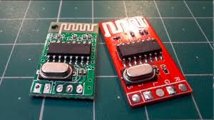
4.2 Chip Antennas
-
Very compact, suitable for IoT
-
Require large ground plane
-
Cost: $0.10–$0.50
-
Require external matching networks
4.3 Patch Antennas
Perfect for GPS, 5G NR, IoT, and small-cell systems.
Support:
-
Linear polarization
-
RHCP / LHCP
-
Dual-polarized configurations
4.4 Whip & Paddle Antennas
-
External, connector-based
-
Used for LoRa, LPWAN, ISM
-
Great modularity
5. RF PCB Antenna Comparison (2.44 GHz)
Property |
IFA |
MIFA |
Chip |
Wire |
|---|---|---|---|---|
| Size (mil) | 157.5×807 | 284×437 | 126×63 | 250×1200 |
| Cost | Minimal | Minimal | $0.10–0.50 | ~$0.10 |
| Bandwidth (MHz, S11 ≤ –10 dB) | 220 | 230 | 200 | 200 |
| Gain (dBi) | 1.1 | 1.6 | 0.5 | 2.0 |
| Best Use | Height-limit designs | Ultra-compact | Tiny IoT nodes | Tall enclosures |
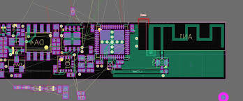
6. RF PCB Layout Guidelines for 5G Devices
1. Place MIMO antennas on PCB corners
Provides isolation, free-space exposure, and reduced mutual coupling.
2. Respect antenna keep-out regions
No metal, vias, components, screws, or traces.
3. Avoid placing antennas near:
-
Batteries
-
LCD modules
-
High-speed processors
-
Switching regulators
-
HDMI or metal shields
4. Use the 8-degree clearance rule
No components should enter the 8° projection boundary around the antenna region.
5. Maintain antenna isolation
-
≥ 10 dB separation below 1 GHz
-
≥ 20 dB for frequencies up to 20 GHz
Use rotation (90°/180°) to maximize orthogonality.
6. Align antenna with final product orientation
Critical for predictable radiation patterns.
7. Avoid metal covers
Metal enclosures detune antennas unless a dedicated RF window is engineered.
8. Keep antennas away from high-εr plastics
Prevents resonant frequency drift and pattern distortion.
