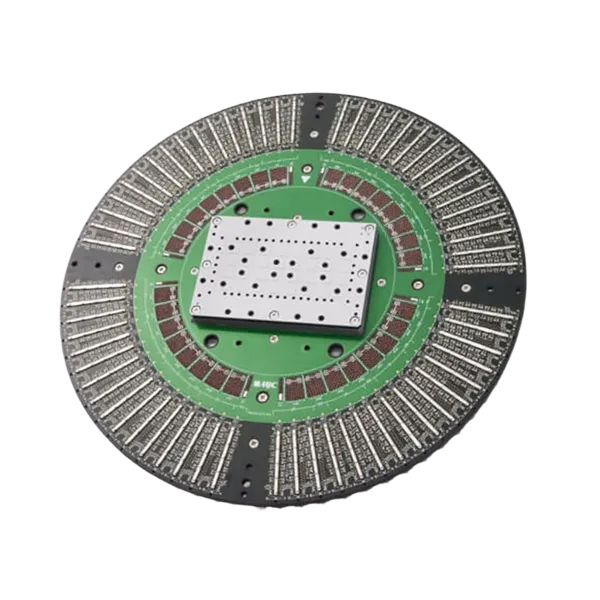
What Makes Probe Card PCBs Unique
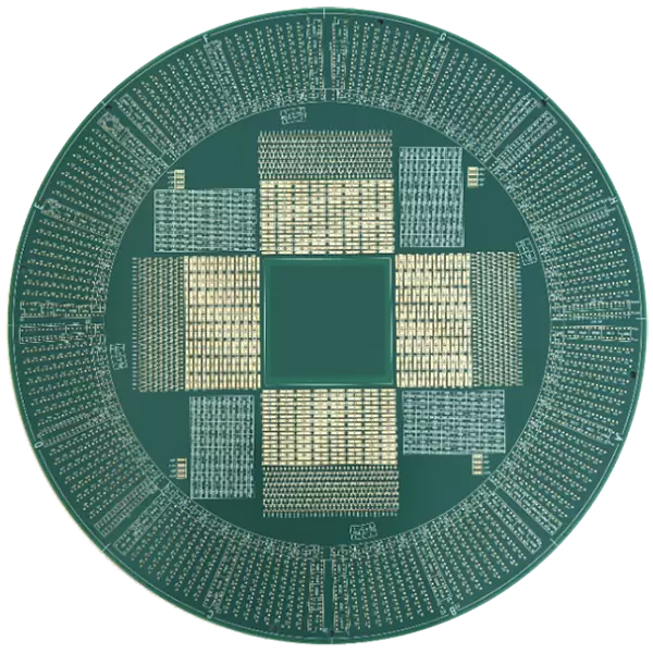
A Probe Card PCB is not a typical circuit board—it is a high-precision interface platform used in semiconductor wafer testing. It connects test equipment (ATE) to microscopic pads on silicon wafers through probe needles or MEMS structures.
Unlike standard PCBs, probe card boards must support:
- Ultra-fine pitch interconnections
- High pin counts (hundreds to thousands of контакts)
- High-frequency signal transmission
- Extremely stable mechanical alignment
This makes probe card PCBs a critical component in ensuring test accuracy, yield optimization, and device reliability during semiconductor manufacturing.
Architecture & Design Logic
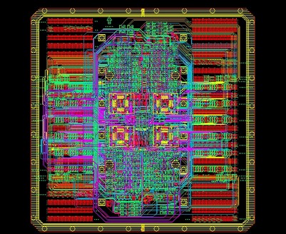
The architecture of a probe card PCB is fundamentally different from conventional designs. It acts as a signal distribution and conditioning platform, bridging large-scale tester interfaces with micro-scale wafer pads.
Key architectural considerations include:
- High-Density Interconnect Routing:
Signals must be routed from dense probe arrays to tester connectors without introducing delay or distortion. - Layer Stack Optimization:
Multilayer structures (often 10–20+ layers) are used to separate signal, ground, and power planes for stability. - Controlled Impedance Paths:
Critical for maintaining signal fidelity, especially in high-speed or RF testing scenarios. - Mechanical Integration:
The PCB must align precisely with probe heads, ensuring accurate contact with wafer pads.
This architecture ensures that the PCB does not become a limiting factor in test precision or repeatability.
Performance & Accuracy Factors
Probe card PCBs directly influence the quality of semiconductor testing. Key performance factors include:
- Signal Integrity (SI):
Minimizing insertion loss, reflection, and crosstalk ensures accurate measurement results. - Contact Stability:
Stable electrical paths between probe needles and PCB traces prevent intermittent failures during testing. - Thermal Stability:
Temperature variations can affect both electrical characteristics and mechanical alignment. - High-Frequency Performance:
Modern semiconductor devices require testing at GHz frequencies, demanding low-loss materials and precise routing. - Repeatability:
Consistent performance across thousands of test cycles is essential for production environments.
Even small inconsistencies can lead to false test results or yield loss, making PCB quality critical.
Manufacturing Challenges
Producing probe card PCBs involves significant technical challenges:
- Ultra-Fine Trace & Pitch Requirements:
Advanced photolithography and etching processes are needed to achieve fine line widths and spacing. - High Layer Count & Registration Accuracy:
Precise alignment across many layers is required to maintain signal integrity and connectivity. - Material Selection:
Low-loss laminates (such as Rogers or PTFE-based materials) are often required for high-frequency testing. - Via Reliability:
Microvias, blind vias, and buried vias must maintain electrical performance under repeated use. - Mechanical Precision:
The PCB must meet strict flatness and tolerance requirements for proper probe alignment. - Quality Assurance:
- Electrical and impedance testing
- X-ray inspection for internal structures
- Thermal and mechanical stress testing
- High-frequency validation (VNA/TDR)
At KKPCB, advanced manufacturing control ensures probe card PCBs meet both electrical precision and mechanical stability requirements.
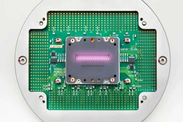
When Should You Use a Probe Card PCB?
Probe card PCBs are essential in semiconductor testing environments where precision and repeatability cannot be compromised:
- Wafer-Level Testing (WLT)
- IC validation and characterization
- High-frequency RF chip testing
- Advanced node semiconductor production
- High-pin-count device testing (SoC, ASIC, memory)
If your application requires accurate signal measurement at scale, a probe card PCB is not optional—it is foundational.
Final Thoughts
Probe card PCBs represent the intersection of precision engineering, high-frequency design, and advanced manufacturing. Their role goes beyond connectivity—they directly impact test accuracy, yield, and production efficiency in semiconductor workflows.
By combining high-density routing, low-loss materials, precise stack-ups, and strict QA processes, KKPCB delivers Probe Card PCBs that support next-generation semiconductor testing with confidence and consistency.
