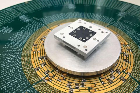
A Probe Card Assembly PCB is a highly specialized semiconductor test PCB used in wafer-level testing to electrically interface between Automated Test Equipment (ATE) and semiconductor wafers. As the core structure of a probe card, this PCB supports probe needles, MEMS probes, or vertical probe arrays, ensuring precise signal transmission and reliable mechanical alignment during IC testing.
With semiconductor devices advancing toward smaller geometries, higher pin counts, and higher test frequencies, the requirements for probe card assembly PCB design and manufacturing have become increasingly stringent. Signal integrity, mechanical precision, and long-term stability are critical for accurate wafer probing.
Key Design Requirements of Probe Card Assembly PCBs
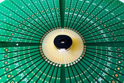
1. Ultra-High Density and Fine-Pitch Routing
Modern wafers feature extremely fine pad pitch. Probe card assembly PCBs use HDI technology, microvias, and fine-line routing to support dense interconnections without signal degradation.
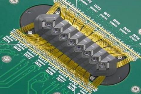
2. Controlled Impedance and Signal Integrity
High-speed digital and RF wafer testing demands strict controlled impedance PCB design. Proper stackup and trace geometry reduce reflection, skew, and insertion loss.
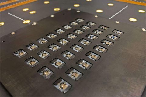
3. Mechanical Accuracy and Flatness Control
Precise planarity is essential to ensure uniform probe contact across the wafer. Tight PCB thickness tolerance and mechanical stability are critical for consistent probing performance.
4. Power Integrity and Low-Noise Design
Stable power delivery ensures accurate parametric testing. Optimized power and ground planes minimize voltage fluctuation and electrical noise during wafer-level measurements.
5. Thermal Stability and Reliability
Wafer testing often involves temperature cycling. High-Tg materials and stable laminates ensure consistent electrical and mechanical performance over repeated test cycles.
Applications of Probe Card Assembly PCBs
Probe card assembly PCBs are widely used in testing:
-
Logic and microprocessor wafers
-
Memory wafers (DRAM, NAND, Flash)
-
RF and mixed-signal semiconductor wafers
-
Advanced packaging and wafer-level ICs
-
Automotive, AI, and high-reliability semiconductor devices
These applications demand extreme accuracy, repeatability, and durability.
Manufacturing Capabilities for Probe Card Assembly PCBs
Producing reliable probe card assembly PCBs requires advanced manufacturing expertise, including:
-
HDI and high-layer-count PCB fabrication
-
Ultra-fine line etching and precision drilling
-
Controlled impedance verification
-
High-Tg and low-loss laminate processing
-
Prototype, small batch, and volume production support
Advanced manufacturing ensures stable performance throughout the probe card lifecycle.
Why Probe Card Assembly PCB Quality Is Critical
Any mechanical or electrical instability in a probe card assembly PCB can lead to poor probe contact, signal distortion, or measurement errors, directly impacting wafer yield and test accuracy. High-quality PCBs deliver:
-
Consistent probe contact across the wafer
-
Accurate high-speed and RF signal measurement
-
Reduced probe card maintenance and downtime
-
Improved wafer test yield and throughput
Conclusion
The Probe Card Assembly PCB is a fundamental element in wafer-level semiconductor testing, providing the electrical and mechanical foundation for accurate IC validation. Through HDI routing, controlled impedance design, mechanical precision, and robust manufacturing, these PCBs ensure reliable and repeatable probe performance.
Partnering with an experienced probe card assembly PCB manufacturer helps improve test accuracy, extend probe card lifespan, and support advanced semiconductor testing requirements.
