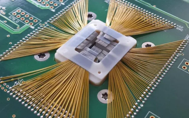
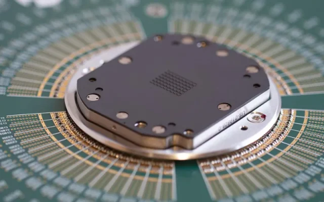
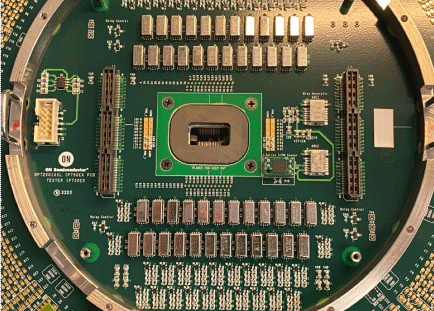
A Probe Card Assembly PCB is a highly specialized printed circuit board used in semiconductor wafer testing, acting as the critical electrical interface between the automated test equipment (ATE) and the device under test (DUT). It enables precise signal transmission from the tester to microscopic probe needles or MEMS probes that contact IC pads on the wafer.
Due to the increasing complexity of semiconductor devices, modern probe card PCBs must support high pin count, ultra-fine pitch, high-speed signals, and high-frequency performance, all while maintaining exceptional mechanical stability and electrical reliability.
Key Design Requirements for Probe Card Assembly PCB
Probe card assembly PCBs face some of the most demanding requirements in PCB manufacturing:
-
High pin count & fine pitch routing for advanced IC nodes
-
Controlled impedance PCB design for high-speed and RF test signals
-
Low loss materials to maintain signal integrity at high frequencies
-
Multilayer and HDI structures to support dense signal routing
-
Tight flatness and planarity control to ensure accurate probe contact
-
Excellent thermal stability for repeated test cycles
These requirements make probe card PCBs fundamentally different from standard test boards or production PCBs.
Materials Used in Probe Card Assembly PCB
Material selection is critical for probe card PCB performance. Commonly used materials include:
-
High-TG FR-4 for general digital IC testing
-
Low Dk / Low Df laminates for high-speed and RF IC test PCB
-
Rogers, Isola, Panasonic, Megtron series for controlled impedance and low loss
-
Hybrid material stackups for mixed-signal probe card designs
For RF IC test PCB and microwave IC test PCB, low loss materials are essential to minimize insertion loss and phase distortion.
Manufacturing Capabilities
A professional Probe Card Assembly PCB manufacturer must support advanced processes such as:
-
HDI PCB fabrication (microvias, laser vias, stacked vias)
-
High layer count PCB (20+ layers for complex ATE systems)
-
Impedance controlled PCB manufacturing with tight tolerance
-
Fine line & space capability for dense probe routing
-
Rigid-flex PCB options for special probe card structures
-
Small batch & prototype production with fast delivery
Strict process control is required to ensure consistency across multiple test cycles and long service life.
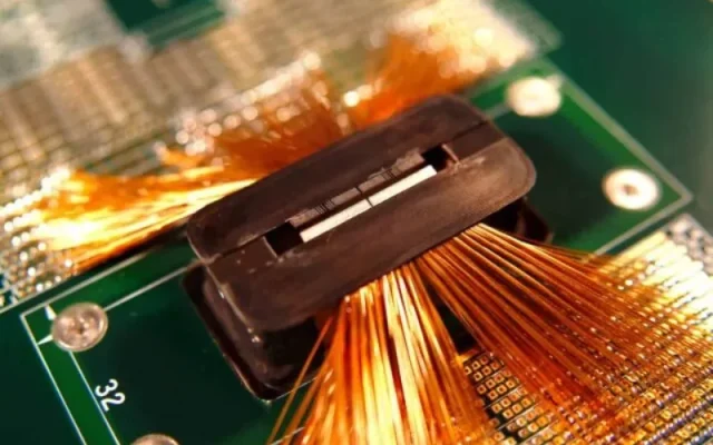
Assembly Considerations for Probe Card PCB
Probe card assembly involves precise integration of:
-
Probe needles or MEMS probes
-
Connectors and sockets
-
High-speed test interfaces
-
RF components (if applicable)
PCB surface finish options such as ENIG, ENEPIG, or hard gold are often selected to enhance wear resistance and contact reliability.
Applications of Probe Card Assembly PCB
Probe card assembly PCBs are widely used in:
-
Wafer test PCB for logic, memory, and mixed-signal ICs
-
IC testing PCB in semiconductor production lines
-
Memory test PCB for DRAM, NAND, and advanced memory devices
-
RF and microwave IC test systems
-
Automated test equipment (ATE) PCB platforms
As semiconductor nodes shrink and frequencies increase, probe card PCB technology continues to evolve rapidly.
Why Choose a Specialized Probe Card PCB Supplier
Working with an experienced probe card assembly PCB supplier ensures:
-
Optimized stackup and impedance control
-
High yield in wafer test environments
-
Stable electrical performance across temperature and frequency
-
Fast prototype support and scalable small batch production
-
Engineering support from DFM to final assembly
This expertise directly impacts test accuracy, throughput, and overall semiconductor manufacturing efficiency.
