
With the continuous development of electronic products toward higher performance, smaller size, higher integration, and improved reliability, traditional PCB manufacturing processes are increasingly unable to meet the requirements of advanced applications.
To achieve specific electrical, mechanical, thermal, and reliability performance, PCB manufacturers have developed various special processing technologies beyond standard fabrication processes.
PCB special processing technologies are mainly applied in areas such as:
- High-density electronic products
- High-frequency communication systems
- Automotive electronics
- Semiconductor testing equipment
- Power electronics
- Medical devices
- Aerospace and industrial control systems
These technologies include:
- HDI microvia processing
- Back drilling technology
- Impedance control processing
- Heavy copper PCB manufacturing
- Laser drilling
- Embedded component technology
- Special surface finishing
- Controlled depth drilling
- High-frequency material processing
This article introduces the major special processing technologies used in PCB manufacturing and explains their applications and key manufacturing considerations.
1. HDI (High Density Interconnect) Processing Technology
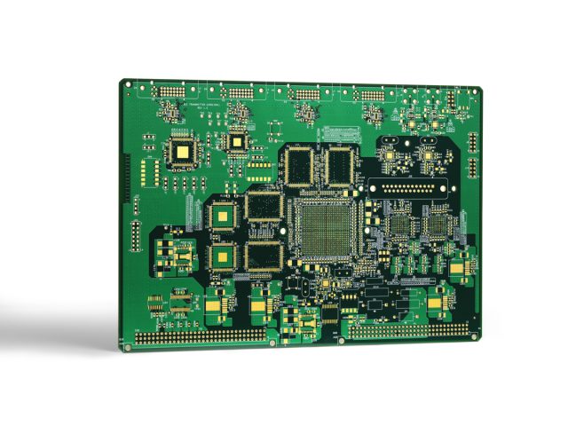
1.1 Overview of HDI Technology
HDI is one of the most important advanced PCB manufacturing technologies.
Unlike traditional PCBs that mainly use mechanical through holes, HDI technology uses:
- Microvias
- Blind vias
- Buried vias
- Fine-line routing
to achieve higher wiring density.
1.2 Advantages of HDI PCB
HDI technology provides:
Higher Integration Density
Allows more circuits within a smaller PCB area.
Applications:
- Smartphones
- Wearable devices
- Medical electronics
- Compact industrial equipment
Improved Signal Performance
Shorter interconnection paths help reduce:
- Signal loss
- Parasitic effects
- Electromagnetic interference
Reduced Product Size
HDI allows:
- Smaller PCB dimensions
- More compact electronic designs
1.3 HDI Manufacturing Considerations
Important process controls include:
- Microvia reliability
- Laser drilling accuracy
- Copper plating quality
- Layer alignment precision
Poor HDI processing may cause:
- Via cracking
- Open circuits
- Reliability failures
2. Laser Drilling Technology
2.1 Principle of Laser Drilling
Laser drilling uses focused laser energy to create extremely small holes in PCB materials.
Compared with mechanical drilling, laser drilling provides:
- Smaller hole diameter
- Higher precision
- Better suitability for fine-pitch designs
2.2 Applications
Laser drilling is widely used in:
- HDI PCBs
- Semiconductor test boards
- High-density communication boards
2.3 Manufacturing Challenges
Laser processing requires precise control of:
- Laser energy
- Drilling depth
- Material properties
Incorrect parameters may cause:
- Resin damage
- Poor via connection
- Reduced reliability
3. Back Drilling Technology
3.1 What Is Back Drilling?
Back drilling is a controlled-depth drilling process used to remove unused portions of through-hole vias.
In high-speed PCB designs, unused via sections can act as:
- Signal reflection points
- Resonant structures
3.2 Advantages of Back Drilling
It helps improve:
- Signal integrity
- High-speed transmission performance
- Impedance stability
Applications:
- Servers
- Data communication equipment
- High-speed computing systems
3.3 Key Process Requirements
Important parameters include:
- Drilling depth accuracy
- Remaining stub length control
- Layer positioning accuracy
4. Controlled Impedance Processing Technology
4.1 Importance of Impedance Control
For high-speed and high-frequency PCBs, impedance consistency directly affects signal quality.
Poor impedance control may result in:
- Signal reflection
- Data errors
- Transmission loss
4.2 Factors Affecting PCB Impedance
Main influencing factors include:
- Trace width
- Copper thickness
- Dielectric thickness
- Material dielectric constant (Dk)
4.3 Manufacturing Requirements
Manufacturers need to control:
- Stack-up structure
- Material parameters
- Etching accuracy
Testing methods include:
- TDR impedance testing
Common requirements:
- 50Ω single-ended impedance
- 90Ω differential impedance
- 100Ω differential impedance
5. Heavy Copper PCB Processing Technology
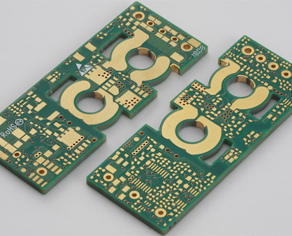
5.1 Overview
Heavy copper PCBs use thicker copper layers to support higher current loads.
Compared with standard copper thickness, heavy copper boards provide:
- Higher current carrying capability
- Better heat dissipation
- Improved mechanical strength
5.2 Applications
Common applications include:
- Power supplies
- Battery management systems
- Motor controllers
- Industrial power equipment
5.3 Manufacturing Challenges
Heavy copper manufacturing requires control of:
- Copper plating uniformity
- Etching accuracy
- Thermal stress
Potential issues include:
- Uneven copper distribution
- Line width deviation
6. Embedded Component Technology
6.1 Concept
Embedded component technology integrates electronic components directly inside the PCB structure.
Components may include:
- Resistors
- Capacitors
- IC devices
6.2 Advantages
Benefits include:
- Reduced PCB size
- Shorter signal paths
- Improved electrical performance
Applications:
- Miniaturized electronics
- High-frequency modules
- Advanced packaging systems
6.3 Challenges
Manufacturing requires:
- High positioning accuracy
- Reliable encapsulation
- Advanced inspection methods
7. High-Frequency PCB Special Processing Technology
7.1 Material Processing
High-frequency PCBs require specialized materials such as:
Important parameters:
- Dielectric constant stability
- Dissipation factor
- Thermal expansion characteristics
7.2 Manufacturing Considerations
Special attention is required for:
- Material handling
- Surface roughness control
- Copper profile control
These factors influence:
- Insertion loss
- Signal delay
- Phase stability
8. Special Surface Treatment Technologies
Surface finishing protects copper surfaces and improves solderability.
Common advanced surface finishes include:
ENIG
Advantages:
- Flat surface
- Good corrosion resistance
- Suitable for fine-pitch components
ENEPIG
Advantages:
- Higher reliability
- Improved wire bonding compatibility
Applications:
- High-reliability electronics
- Semiconductor-related products
Immersion Silver
Advantages:
- Good electrical performance
- Suitable for high-frequency applications
9. Controlled Depth Drilling Technology
Controlled depth drilling allows holes to stop at a specific layer.
Applications include:
- Blind vias
- Special mechanical structures
- High-density PCB designs
Advantages:
- Improved routing flexibility
- Reduced board thickness
- Better space utilization
10. Flexible and Rigid-Flex PCB Processing
Rigid-flex PCB technology combines:
- Rigid PCB sections
- Flexible circuit sections
Special processing includes:
- Flexible material lamination
- Coverlay processing
- Stiffener bonding
- Precision alignment
Advantages:
- Reduced connectors
- Improved reliability
- Space optimization
Applications:
- Medical devices
- Aerospace electronics
- Wearable products
11. PCB Special Testing Technologies
Advanced PCB manufacturing requires specialized testing.
AOI Inspection
Detects:
- Circuit defects
- Pattern abnormalities
X-Ray Inspection
Used for:
- Hidden structures
- BGA connections
- Internal defects
TDR Testing
Used for:
- Impedance measurement
- High-speed signal verification
Reliability Testing
Includes:
- Thermal cycling
- Mechanical stress testing
- Humidity testing
12. Future Development Trends of PCB Special Processing
With increasing demands for advanced electronics, PCB processing technologies are developing toward:
Higher Density
Driven by:
- Smaller electronic products
- Advanced semiconductor packages
Higher Speed
Driven by:
- 5G communication
- High-performance computing
- AI hardware
Higher Reliability
Driven by:
- Automotive electronics
- Industrial systems
- Medical applications
Conclusion
PCB special processing technologies provide essential support for modern electronic products requiring advanced performance and reliability.
Technologies such as:
- HDI microvia processing
- Laser drilling
- Back drilling
- Controlled impedance manufacturing
- Heavy copper processing
- High-frequency material processing
- Rigid-flex manufacturing
enable PCBs to achieve higher integration, faster signal transmission, improved thermal performance, and stronger reliability.
As electronic systems continue moving toward higher speed, smaller size, and greater complexity, advanced PCB processing technologies will remain a key foundation for next-generation electronic innovation.
