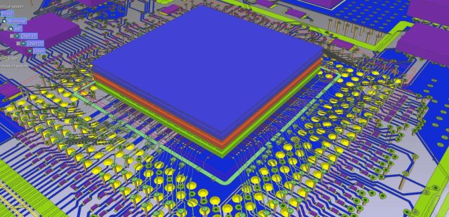
A Package Test PCB is a specialized semiconductor test PCB used to validate ICs at the package level, ensuring electrical performance, mechanical integrity, and reliability before final product deployment. These boards serve as the interface between packaged ICs and Automated Test Equipment (ATE), enabling functional, parametric, and stress testing across various package formats.
As semiconductor packages continue to evolve toward smaller footprints, finer pitches, and higher pin counts, package test PCBs play a critical role in delivering accurate, repeatable test results and ensuring product quality.
Key Design Requirements for Package Test PCBs
1. Compatibility with Multiple Package Types
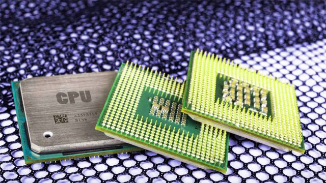
Package test PCBs must support a wide range of IC packages, including BGA, QFN, QFP, LGA, CSP, and advanced system-in-package (SiP) formats.
2. High Pin Count and Fine-Pitch Routing
Modern IC packages often feature hundreds or thousands of pins, requiring HDI technology, microvias, fine-line routing, and multilayer stackups to ensure reliable signal access.
3. Controlled Impedance and Signal Integrity
Accurate testing of high-speed and high-frequency ICs requires precise impedance control, trace length matching, and low crosstalk design to maintain signal integrity.
4. Mechanical Accuracy and Flatness
Package test PCBs must maintain tight mechanical tolerances and excellent flatness to ensure stable socket contact and minimize intermittent test failures.
5. Robust Power and Ground Design
An optimized power distribution network (PDN) ensures stable voltage delivery and minimizes noise during sensitive package-level testing.
Applications of Package Test PCBs
Package test PCBs are widely used in:
-
Final test and validation of packaged ICs
-
High-speed logic and processor package testing
-
Memory and storage IC package validation
-
RF and mixed-signal IC package testing
-
Automotive and industrial semiconductor qualification
These applications demand high accuracy, repeatability, and reliability in test results.
Manufacturing Requirements for Package Test PCBs
Producing high-quality package test PCBs requires advanced PCB manufacturing capabilities, including:
-
Multilayer and HDI PCB fabrication
-
Fine-line etching and microvia processing
-
Controlled impedance testing and verification
-
Tight dimensional tolerance and flatness control
-
Prototype, small batch, and volume production support
These processes ensure consistent electrical performance and dependable testing outcomes.
Why Package Test PCB Quality Matters
Inferior package test PCBs can lead to:
-
Unstable socket contact and intermittent signals
-
Measurement inaccuracies and false test failures
-
Reduced test yield and longer validation cycles
-
Increased production costs and equipment downtime
High-quality Package Test PCBs ensure accurate validation, improved yield, and reliable semiconductor package testing.
Conclusion
The Package Test PCB is a vital component in semiconductor manufacturing and quality assurance, enabling accurate validation of IC packages before mass production. Through HDI routing, controlled impedance design, mechanical precision, and robust power distribution, these boards deliver reliable performance in demanding ATE environments.
Partnering with an experienced package test PCB manufacturer ensures high-quality test solutions that support faster validation cycles, higher yield, and long-term reliability.
