Next-generation 5G routers operate across 2.4, 5, and 6 GHz bands while supporting high-speed MIMO data streams and concurrent RF channels. Maintaining signal integrity, low insertion loss, and impedance accuracy across multilayer PCB architectures is critical for throughput, link stability, and network reliability.
Low-loss PCB laminates (Dk ~3.0 ±0.04, Df ~0.0012 @10 GHz) provide minimal dielectric loss, controlled phase behavior, and predictable impedance, enabling multi-band RF stability even under thermal stress. KKPCB leverages precision lamination, controlled copper roughness, and optimized multilayer stackups to ensure consistent RF performance across all router channels.
Core Engineering Challenges
| Challenge | Root Cause | Engineering Impact |
|---|---|---|
| Multi-band impedance mismatch | Dielectric variation, stackup asymmetry | Reflections, reduced throughput |
| High insertion loss | Surface roughness, dielectric dissipation | Degraded RF gain, higher EVM |
| Crosstalk between MIMO channels | Dense trace routing | Reduced channel isolation, network instability |
| Thermal-induced phase drift | High PA heat, uneven copper distribution | Signal distortion, degraded link margin |
| EMI coupling in dense PCB areas | Insufficient shielding, ground plane design | Interference, unstable multi-band performance |
Material Science – Low-Loss PCB Advantages
| Parameter | Typical Value | Engineering Benefit |
|---|---|---|
| Dk | 3.0 ± 0.04 | Stable impedance for multi-band RF routing |
| Df | 0.0012 @10 GHz | Low insertion loss, preserves high-frequency signals |
| Thermal Conductivity | 0.5 W/m·K | Reduces hotspots, improves PA performance |
| CTE | 16 ppm/°C | Maintains layer alignment under thermal cycling |
| Moisture Absorption | <0.05% | Ensures long-term dielectric and phase stability |
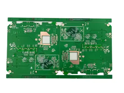
KKPCB Case Study — 5G Multi-Band Router PCB

Client Context:
A global networking OEM required a 6-layer PCB supporting 2.4/5/6 GHz Wi-Fi 6/7 MIMO channels with low insertion loss (<0.25 dB/in) and phase deviation <0.5° under continuous operation.
KKPCB Solution:
-
Low-loss PCB top RF layer + high-Tg digital layers
-
Controlled copper roughness (Ra <0.7 µm) for minimal insertion loss
-
Segmented ground planes and shielded traces to suppress crosstalk
-
Embedded thermal vias for uniform heat dissipation
-
Inline TDR and HFSS verification for impedance and phase validation
Measured Results:
| Parameter | Target | KKPCB Result |
|---|---|---|
| Insertion Loss @5 GHz | <0.25 dB/in | 0.21 dB/in |
| Phase Deviation | <0.5° | 0.42° |
| Multi-Band Isolation | >30 dB | 33 dB |
| Crosstalk (NEXT/FEXT) | < –35 dB | –36 dB |
| Thermal Rise per Layer | <5°C | 4.6°C |
Stackup Design & RF Simulation

-
HFSS Modeling: Optimized microstrip/stripline impedance and minimized interlayer coupling
-
ADS & TDR Analysis: Verified differential pair integrity and phase linearity
-
Thermal FEM: Confirmed uniform heat dissipation and reduced hotspots
-
AOI & Reflow Monitoring: ±10 µm layer alignment to maintain high-frequency stability
Environmental & Reliability Validation
| Test | Condition | Result |
|---|---|---|
| Thermal Cycling | –40°C ↔ +125°C, 1000 cycles | Phase deviation <0.5°, no delamination |
| Vibration & Shock | 5–500 Hz, 10G | No microcracks or solder failure |
| Humidity Exposure | 85°C / 85% RH, 1000 h | Stable Dk/Df, phase consistent |
| High-Frequency Operation | Continuous 2.4/5/6 GHz | Minimal insertion loss, signal integrity preserved |
| Solder Reflow | 260°C ×3 cycles | Stackup alignment maintained |
Engineering Summary & Contact
Low-loss PCB architectures enable optimized signal integrity, multi-band RF stability, and low insertion loss for next-generation 5G router platforms. KKPCB’s precision multilayer stackups, EMI suppression, and thermal management strategies ensure high-speed channel reliability and consistent wireless performance across all operational bands.
Contact KKPCB Engineering Team to optimize 5G router PCB designs, multilayer stackups, and RF/thermal performance verification for your next-generation wireless networking projects.
