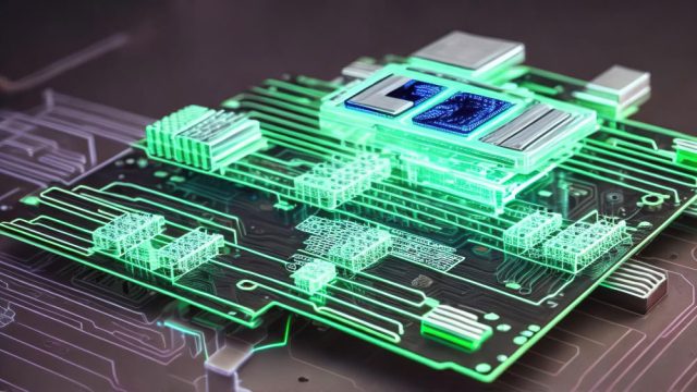
Modern electronic testing systems demand accurate signal transmission, stable power delivery, and repeatable results. The Multilayer Test PCB is specifically designed to meet these requirements by integrating multiple signal, power, and ground layers into a compact and electrically optimized structure.
A well-designed multilayer test PCB ensures consistent and reliable test performance.
What Is a Multilayer Test PCB?
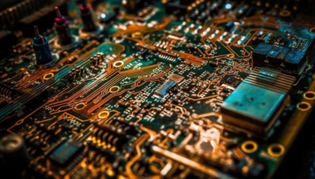
A Multilayer Test PCB is a printed circuit board that uses three or more conductive layers to support complex test signal routing, power distribution, and grounding schemes. Unlike standard PCBs, test PCBs must deliver precise and repeatable electrical behavior.
Why Multilayer Structures Are Essential for Test PCBs
Multilayer architectures enable:
-
Dedicated signal layers for clean routing
-
Continuous reference planes for impedance control
-
Isolated power layers for stable voltage delivery
These benefits are critical in high-accuracy test applications.
Signal Integrity in Multilayer Test PCBs
Maintaining signal integrity is a primary design goal. Multilayer test PCBs focus on:
-
Controlled impedance transmission lines
-
Short and direct signal paths
-
Reduced crosstalk through layer separation
These techniques ensure accurate signal measurement.
Power and Ground Plane Design
Reliable testing requires clean power and grounding. Multilayer test PCBs typically include:
-
Solid ground planes for low noise
-
Multiple power planes for different voltage domains
-
Optimized return paths to minimize EMI
Proper plane design enhances test stability.
Stackup Design and Layer Optimization
Effective stackup design considers:
-
Signal-to-plane adjacency
-
Symmetrical layer distribution
-
Thermal and mechanical stability
A balanced stackup improves manufacturability and long-term reliability.
Material Selection for Test Accuracy
Multilayer test PCBs may use:
-
High-Tg FR-4 for dimensional stability
-
Low-loss laminates for high-speed signals
-
Mixed material stackups for cost-performance balance
Material choice directly impacts signal quality.
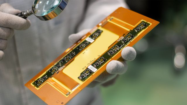
Manufacturing Precision and Quality Control
Test PCBs require strict manufacturing control, including:
-
Tight layer registration
-
Consistent copper thickness
-
Electrical testing and impedance verification
Precision manufacturing ensures repeatable test results.
Applications of Multilayer Test PCBs
Multilayer test PCBs are commonly used in:
-
Automated test equipment (ATE)
-
Semiconductor device testing
-
Load boards and interface boards
-
Functional and validation test systems
Each application relies on consistent electrical behavior.
Choosing a Multilayer Test PCB Manufacturer
When selecting a multilayer test PCB supplier, evaluate:
-
Experience in test and validation PCBs
-
Controlled impedance fabrication capability
-
Support for prototype and low-volume builds
-
Engineering assistance during DFM review
The right partner improves yield and test accuracy.
Conclusion
The Multilayer Test PCB is a critical component in advanced electronic testing systems. By combining optimized layer stackups, stable power distribution, and controlled signal routing, multilayer test PCBs deliver accurate, repeatable, and reliable test performance.
Partnering with an experienced multilayer test PCB manufacturer ensures high-quality boards that meet demanding test requirements.
