What Is a Multilayer HF PCB?
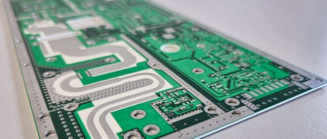
A Multilayer HF PCB is a printed circuit board with three or more layers designed specifically for high-frequency (HF) and RF signal transmission. These PCBs combine high-speed digital and RF design requirements with multilayer routing, providing:
-
High signal density
-
Controlled impedance
-
Low-loss transmission
-
Enhanced EMI/EMC performance
They are widely used in 5G routers, radar modules, mmWave sensors, and high-speed communication devices.
Key Features of Multilayer HF PCB
High-performance multilayer HF PCBs have several distinguishing features:
-
Low dielectric loss materials for minimal signal attenuation
-
Precise impedance control for high-speed and RF traces
-
Optimized multilayer stack-up to minimize crosstalk and signal degradation
-
Thermal management for power and RF components
-
Reliable interlayer vias and blind/buried vias
These features ensure stable signal integrity and low insertion loss.
Material Selection for Multilayer HF PCB
Choosing the right material is critical for multilayer HF performance:
-
RO4350B PCB / RF-35 PCB – Low-loss RF laminates
-
Megtron 7 PCB – Ultra-low loss for high-speed digital and mmWave applications
-
Hybrid FR-4 + high-frequency laminates – Cost-effective multilayer solutions
-
Ceramic / Alumina PCB options – For extreme thermal or high-reliability applications
Material selection directly impacts signal integrity, insertion loss, and thermal stability.
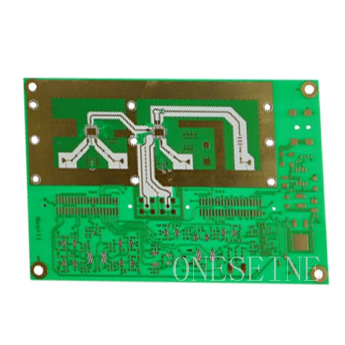
Design Considerations for Multilayer HF PCB
Designing a multilayer HF PCBs requires careful attention:
-
Controlled impedance microstrip and stripline traces
-
Optimized layer stack-up for signal, power, and ground
-
Blind and buried vias for dense multilayer routing
-
Via shielding and isolation to reduce crosstalk
-
Connector launch optimization for RF modules
-
Thermal paths and heat dissipation for active components
Proper design ensures reliable high-frequency performance even in compact multilayer PCBs.
Manufacturing Requirements for Multilayer HF PCB
Producing high-quality multilayer HF PCBs involves:
-
Tight dielectric and layer thickness tolerances
-
Precise registration for multilayer alignment
-
Controlled copper roughness and plating
-
Advanced lamination and drilling processes
-
Comprehensive impedance and RF testing
Expert manufacturers are critical to ensure low insertion loss and repeatable high-frequency performance.
Applications of Multilayer HF PCB
Multilayer HF PCBs are used in:
-
5G router and mmWave communication modules
-
Automotive radar and ADAS sensor systems
-
High-frequency test boards and RF measurement equipment
-
High-speed networking and computing devices
-
IoT gateways and industrial sensor systems
They are essential wherever high-density, high-speed, and low-loss multilayer routing is required.
Conclusion
A Multilayer HF PCB provides a robust platform for high-frequency and high-speed applications, combining low-loss materials, precise impedance control, and optimized multilayer design. Choosing an experienced multilayer HF PCB manufacturer ensures signal integrity, reliability, and consistent performance from prototype to volume production.
