A Mixed Signal IC Test PCB is a specialized semiconductor test PCB designed to validate integrated circuits that combine analog circuits and digital logic on a single chip. These ICs are widely used in power management, sensor interfaces, data converters, automotive electronics, industrial control, and communication systems.
Because mixed signal ICs process both low-level analog signals and high-speed digital signals, their testing environment must be carefully engineered. The test PCB plays a critical role in maintaining signal integrity, noise isolation, and measurement accuracy when interfacing with Automated Test Equipment (ATE).
Why Mixed Signal IC Testing Is More Challenging
Unlike purely digital or analog ICs, mixed signal devices require test boards that can handle:
-
Sensitive analog measurements
-
Fast digital switching and clock signals
-
Noise coupling between analog and digital domains
-
High pin count and fine-pitch packages
A poorly designed test PCB can introduce noise, crosstalk, and measurement errors, leading to false failures or reduced test yield.
Key Design Considerations for Mixed Signal IC Test PCBs
1. Analog and Digital Domain Isolation
Proper separation of analog ground and digital ground, combined with controlled return paths, minimizes noise coupling and improves measurement stability.
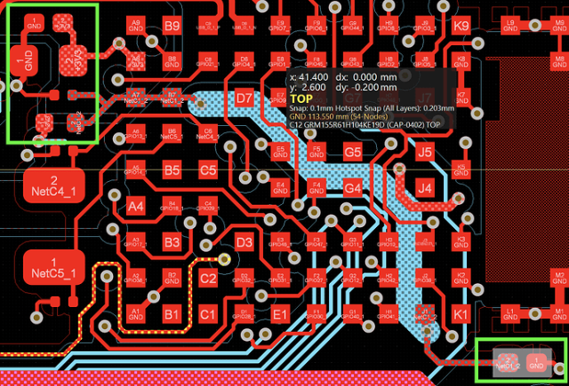
2. Controlled Impedance and High-Speed Routing
Digital interfaces and clock signals require precise controlled impedance routing, trace length matching, and impedance consistency to ensure accurate timing and signal integrity.
3. Low-Noise Power Distribution Network (PDN)
A robust PDN with effective decoupling, local bypass capacitors, and low-impedance planes ensures clean power delivery for sensitive analog blocks.
4. High Pin Count and HDI Routing
Mixed signal ICs often use high pin count packages, requiring HDI technology, microvias, fine-line routing, and multilayer stackups to maintain reliable electrical access.
5. Mechanical Stability and Repeatability
Stable PCB materials and precise manufacturing ensure consistent socket contact and repeatable results over repeated test cycles.
Applications of Mixed Signal IC Test PCBs
Mixed signal IC test PCBs are widely used in:
-
ADC and DAC testing
-
Power management IC (PMIC) validation
-
Sensor interface and signal conditioning IC testing
-
Automotive mixed signal IC qualification
-
Industrial and communication IC validation
These applications demand high accuracy, low noise, and repeatable test performance.
Manufacturing Requirements for Mixed Signal IC Test PCBs
Producing high-quality mixed signal test PCBs requires advanced manufacturing capabilities, including:
-
Multilayer and HDI PCB fabrication
-
Fine-line etching and microvia processing
-
Controlled impedance verification
-
Strict noise and crosstalk control
-
Support for prototype, small batch, and volume production
Tight process control ensures consistent electrical characteristics and reliable test performance.
Why Mixed Signal IC Test PCB Quality Matters
Low-quality test boards can lead to:
-
Increased noise and unstable analog measurements
-
Crosstalk between analog and digital signals
-
Inconsistent test results and reduced yield
-
Longer debug cycles and higher test costs
A professionally engineered Mixed Signal IC Test PCB ensures accurate validation, faster debugging, and reliable production testing.
Conclusion
The Mixed Signal IC Test PCB is essential for validating today’s highly integrated ICs that combine analog precision with digital speed. With optimized layout techniques, controlled impedance routing, low-noise power design, and HDI manufacturing, these boards deliver reliable and repeatable performance in demanding ATE environments.
Working with an experienced mixed signal IC test PCB manufacturer helps ensure high test accuracy, improved yield, and long-term reliability across semiconductor applications.
