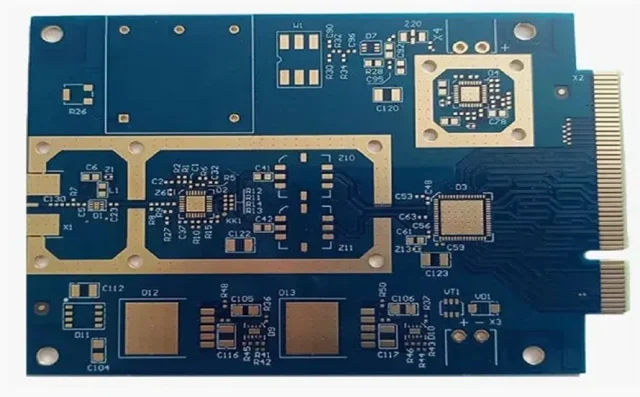
Microwave IC Test PCB: High-Frequency Solutions for Accurate Microwave Chip Testing
With the rapid development of mmWave, 5G, and advanced RF systems, accurate testing of microwave ICs is essential to ensure performance, yield, and reliability. Microwave IC Test PCBs act as the critical interface between microwave chips and automated test equipment (ATE) or probe cards, providing high-density signal routing, controlled impedance, and precise mechanical alignment for reliable testing.
High-quality microwave IC test PCBs enable engineers to perform functional, parametric, and wafer-level testing efficiently, reducing errors and accelerating time-to-market for high-frequency ICs.
What Is a Microwave IC Test PCB?
A Microwave IC Test PCB is a specialized PCB designed for testing high-frequency RF and microwave integrated circuits. Its main functions include:
-
Routing high-frequency signals from IC pads to ATE or probe card interfaces
-
Maintaining controlled impedance and low insertion loss for mmWave and microwave signals
-
Supporting fine-pitch, high-pin-count microwave IC packages
-
Providing mechanical stability for probe alignment
-
Ensuring repeatable, high-accuracy test results
These PCBs are engineered for high-frequency performance, repeatability, and reliability.
Key Features of Microwave IC Test PCBs
-
Low-Loss Signal Routing
Uses advanced materials and trace design to minimize insertion loss at microwave frequencies. -
Controlled Impedance
Maintains signal integrity for high-speed RF and microwave signals to ensure accurate measurements. -
High-Density Routing and Multilayer HDI Design
Supports complex ICs with large pin counts and high-speed traces. -
Mechanical Precision
Ensures consistent probe card alignment and prevents pad damage during repeated test cycles. -
Thermal and Electrical Reliability
Supports burn-in testing, high-current, and long-duration microwave IC validation.
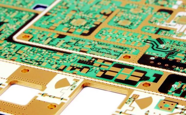
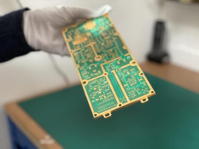
Materials and Stackup Considerations
Selecting the right materials and stackups is critical for microwave IC test PCBs:
-
Low-Loss Laminates (e.g., Rogers, Taconic RF-35, Duroid 5880/6002) for minimal signal attenuation
-
High-Tg FR-4 for mixed-signal applications
-
Hybrid Stackups combining FR-4 and low-loss RF cores for optimized signal integrity
-
Thermally Stable Materials for long-duration burn-in and high-power testing
The right combination of materials and stackup ensures consistent high-frequency performance, signal integrity, and mechanical stability.
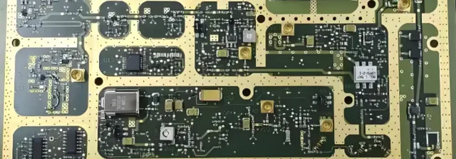
Applications of Microwave IC Test PCBs
Microwave IC test PCBs are widely used in:
-
5G, mmWave, Wi-Fi, and other RF IC functional and parametric testing
-
Wafer-level and package-level microwave IC validation
-
Load boards and probe card interfaces for ATE systems
-
Prototype testing for high-frequency RF and microwave chips
-
Small-batch and pilot production IC validation
These applications demand precision, controlled impedance, and repeatable results—all provided by specialized microwave IC test PCBs.
Choosing a Microwave IC Test PCB Manufacturer
When selecting a microwave IC test PCB supplier, consider:
-
Expertise in high-frequency, controlled-impedance PCB design
-
Ability to manufacture HDI, multilayer, and high-pin-count boards
-
Experience with low-loss RF and microwave materials
-
Support for prototype, small-batch, and volume production
-
Strong engineering and quality assurance processes
A professional partner ensures accurate, repeatable microwave IC testing and reduces development risk.
Conclusion
Microwave IC Test PCBs are essential for validating high-frequency ICs, providing low-loss routing, controlled impedance, and mechanical precision. Partnering with an experienced manufacturer ensures reliable microwave IC testing, faster design validation, and seamless transition from prototype to volume production in RF and mmWave applications.
