As memory devices evolve toward higher speeds, greater capacity, and more complex architectures, Memory Test PCBs have become essential for ensuring IC functionality, yield, and reliability. These specialized PCBs act as the interface between memory chips and automated test equipment (ATE), providing high-density signal routing, controlled impedance, and precise mechanical alignment for accurate memory validation.
With reliable memory test PCBs, engineers can efficiently perform functional testing, parametric measurement, and burn-in validation, reducing errors and accelerating product development.
What Is a Memory Test PCB?
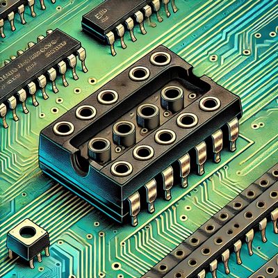
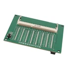
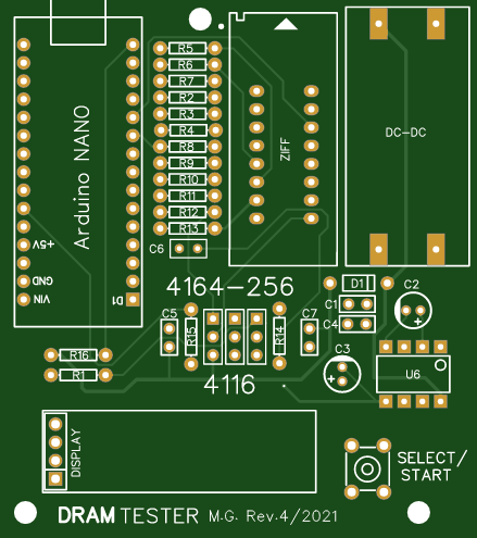
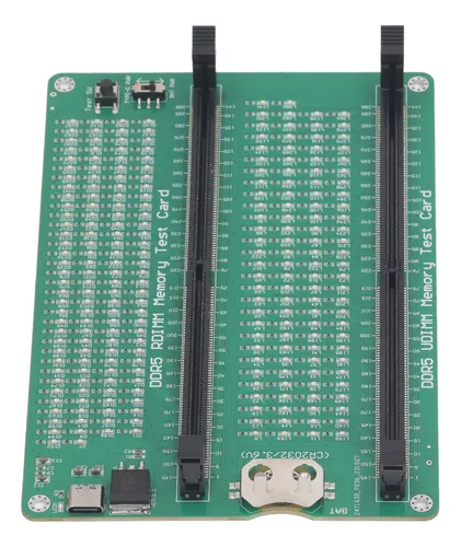
A Memory Test PCB is a printed circuit board designed specifically to test memory ICs such as DRAM, SRAM, and Flash. Key functions include:
-
Routing high-density signals from memory pads to ATE systems
-
Maintaining controlled impedance for high-speed memory signals
-
Supporting high pin count modules and fine-pitch packages
-
Providing mechanical stability for probe alignment and repeated testing
Memory test PCBs ensure accurate, repeatable, and reliable testing across different memory types.
Key Features of Memory Test PCBs
-
High-Speed Signal Integrity
Controlled impedance and low-loss materials preserve memory signal fidelity and minimize reflections. -
High Pin Count Support
Supports memory modules with hundreds or thousands of connections, including DRAM, SRAM, and Flash ICs. -
Multilayer Stackups
Separates power, ground, and signal layers to reduce noise and crosstalk. -
Mechanical Stability and Thermal Reliability
Ensures accurate probe alignment and prevents warping during high-current or burn-in testing. -
Prototype and Small-Batch Flexibility
Rapidly manufactured small-batch memory test PCBs allow design validation before large-scale production.
Material and Stackup Considerations
Memory test PCBs often require specialized materials to meet high-speed and high-frequency requirements:
-
High-Tg FR-4 – Suitable for general memory testing
-
Low-Loss Laminates – Required for high-speed DRAM and Flash validation
-
Hybrid Stackups – Combine FR-4 and low-loss cores for optimized performance
-
Thermal Management Materials – Ensure dimensional stability during prolonged burn-in testing
Proper material and stackup selection ensures signal integrity, mechanical reliability, and repeatable results.
Applications of Memory Test PCBs
Memory test PCBs are widely used in:
-
DRAM, SRAM, and Flash IC functional testing
-
Wafer-level and package-level ATE testing
-
Load boards and test sockets for automated memory test systems
-
Prototype testing for new memory products
-
Small batch and pilot production validation
These applications benefit from high-density routing, controlled impedance, and precise mechanical alignment, improving test accuracy and yield.
Choosing a Memory Test PCB Manufacturer
When selecting a memory test PCB supplier, consider:
-
Experience with high-speed, high-pin-count, and multilayer PCB design
-
Capability for controlled impedance and low-loss routing
-
Support for prototype, small-batch, and volume production
-
Electrical testing, quality control, and thermal verification capabilities
-
Responsive engineering support for design iteration and optimization
A professional partner ensures reliable, repeatable memory testing and reduces time-to-market for memory IC products.
Conclusion
Memory Test PCBs are essential for modern semiconductor memory validation, offering high-density routing, controlled impedance, and mechanical stability for ATE and wafer-level testing. By partnering with an experienced memory test PCB manufacturer, engineers can ensure accurate, reliable, and high-speed memory testing, faster design validation, and smoother transition to full-scale production.
