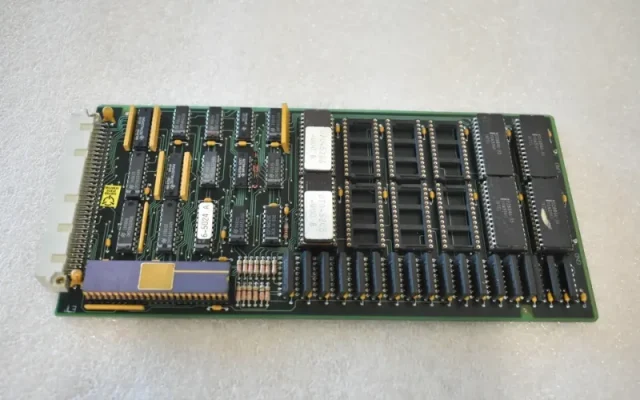
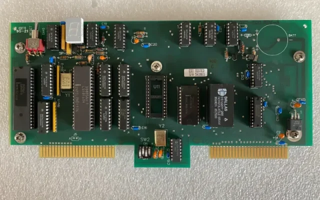
A Memory Test PCB is a specialized semiconductor test board used in Automated Test Equipment (ATE) to evaluate the performance, reliability, and electrical characteristics of memory devices such as DRAM, NAND Flash, NOR Flash, and emerging memory technologies. These test PCBs play a critical role in memory chip validation, characterization, and high-volume production testing.
As memory devices continue to evolve toward higher density, faster data rates, and lower operating voltages, the design and manufacturing requirements for memory test PCBs have become increasingly complex. Accurate testing depends on precise signal integrity, power stability, and robust PCB construction.
Key Design Requirements of Memory Test PCBs
1. High Pin Count and Dense Routing
Modern memory devices feature high I/O counts and fine-pitch packages. Memory test PCBs rely on HDI structures, microvias, and multilayer stackups to support dense routing without compromising electrical performance.
2. Controlled Impedance for High-Speed Interfaces
High-speed memory interfaces such as DDR, LPDDR, and high-bandwidth memory (HBM) require strict controlled impedance PCB design to minimize signal reflection, skew, and timing errors during testing.
3. Power Integrity and Low-Noise Design
Memory devices are highly sensitive to power fluctuations. Optimized power and ground planes, effective decoupling, and low-impedance PDN design ensure stable voltage delivery and accurate test results.
4. Signal Timing and Crosstalk Control
High-speed parallel memory buses demand careful length matching and isolation. Proper spacing, shielding, and stackup design reduce crosstalk and improve timing margin during memory testing.
5. Mechanical Stability and Socket Compatibility
Memory test PCBs must maintain precise alignment with test sockets, load boards, or probe interfaces, ensuring consistent electrical contact during repeated test cycles.
Applications of Memory Test PCBs
Memory test PCBs are widely used for testing:
-
DRAM and LPDDR memory devices
-
NAND and NOR Flash memory
-
Embedded and automotive memory ICs
-
High-speed server and data center memory
-
Emerging non-volatile memory technologies
These applications require high accuracy, repeatability, and long-term reliability in semiconductor test environments.
Manufacturing Capabilities for Memory Test PCBs

Producing reliable memory test PCBs requires advanced manufacturing capabilities, including:
-
HDI and high-layer-count PCB fabrication
-
Controlled impedance manufacturing and verification
-
Fine-line etching and precision drilling
-
High-Tg and low-loss laminate processing
-
Prototype, small batch, and volume production support
Advanced manufacturing ensures consistent performance and repeatable testing results.
Why Memory Test PCB Quality Is Critical
Low-quality memory test PCBs can introduce signal distortion, power noise, and timing instability, leading to inaccurate test results and reduced yield. High-performance test boards ensure:
-
Accurate memory speed and timing validation
-
Stable power delivery during high-speed operation
-
Reduced test errors and rework
-
Improved ATE efficiency and throughput
Conclusion
The Memory Test PCB is a fundamental component of memory semiconductor testing, enabling accurate evaluation of high-speed, high-density memory devices. Through HDI routing, controlled impedance design, robust power integrity, and precise manufacturing, memory test PCBs deliver reliable and repeatable test performance.
Partnering with an experienced memory test PCB manufacturer ensures consistent quality, faster test development, and dependable results throughout memory chip production.
