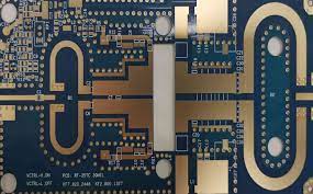
High-frequency signal integrity is the defining performance factor in modern 5G mmWave antenna systems, where routing density, insertion loss, and phase stability determine overall RF efficiency. As 5G architectures transition to 26–29 GHz, 37–40 GHz, and 60 GHz mmWave bands, the electrical behavior of the Low Loss PCB stackup becomes just as important as the antenna design itself. Any deviation in dielectric properties, copper roughness, or interconnect geometry directly impacts mmWave PCB losses, beamforming precision, and EVM performance.
To meet these requirements, Low Loss PCB laminates—such as RO4350B, RO3003, RO4835, and PTFE-based RF materials—provide ultra-stable Dk/Df characteristics engineered for high-frequency and mmWave propagation. Their predictable dielectric behavior ensures that 5G mmWave antenna modules maintain phase coherence, low attenuation, and reliable RF performance across wideband operating ranges.
Why Low Loss PCB Laminates Determine mmWave Antenna Quality
1. Ultra-Low Dielectric Loss for Clean mmWave Routing
In mmWave networks, even a small increase in dielectric loss degrades the signal chain.
Low Loss PCB materials maintain extremely low Df across 28–40 GHz, reducing attenuation in:
• mmWave antenna feed networks
• Beamforming distribution layers
• High-frequency phase shifters
• CPW and microstrip transmission lines
• RF front-end routing paths
Their stable dielectric properties ensure accurate impedance and controlled propagation velocity.
2. High-Frequency Phase Stability for Beamforming Arrays
Beamforming accuracy depends on consistent RF phase performance.
Low Loss PCB laminates deliver:
• Tight Dk tolerance
• Low TCDk for thermal stability
• Minimal material dispersion
This directly enhances 5G mmWave antenna phase alignment, radiation efficiency, and multi-element coherence.
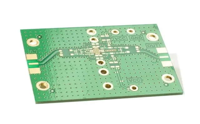
3. Low-Loss Interconnects for High-Density RF Modules
mmWave PCB structures rely on precise interconnect geometry.
KKPCB optimizes:
• Microstrip / CPW transitions
• Via-in-pad RF interconnects
• Copper roughness control
• Ultra-thin dielectric spacing
• Controlled impedance traces at 50 Ω
These reduce conductor loss, maintain high-frequency linearity, and improve mmWave S-parameters.
Engineered mmWave PCB Stackups for 5G Antenna Systems
Advanced mmWave PCB stackups combine hybrid material systems—PTFE, hydrocarbon-ceramic composites, and low-loss bonding films—to maintain high-frequency uniformity.
KKPCB designs stackups that include:
• Dedicated low-loss RF layers for antenna feed networks
• Hybrid digital + RF PCB structures
• Controlled dielectric thickness for stable impedance
• Air-cavity or low-Dk regions for radiation apertures
• High-density blind/laser microvias for compact mmWave arrays
These stackups allow antenna modules to support high-power beamforming, tighter phase matching, and wider bandwidth.
High-Frequency Manufacturing Techniques for Low Loss PCB Reliability
High-frequency reliability requires precise mmWave PCB fabrication.
KKPCB integrates:
• Laser microvias for minimal mmWave via stubs
• Low-profile copper (HVLP/EDLP) to reduce conductor loss
• Controlled etching to maintain critical trace widths
• Vacuum lamination for Dk uniformity
• RF shielding structures for EMI suppression
• Resin-filled via-in-pad for dense phased-array packaging
This ensures Low Loss PCB performance remains consistent from prototype to mass production.
Applications Across 5G mmWave Antenna Platforms
Low Loss PCB laminates are fundamental to every generation of mmWave antenna systems, including:
• 5G mmWave base stations (28 / 39 GHz)
• mmWave CPE terminals
• Smartphone mmWave antenna-in-package (AiP) modules
• High-density phased-array tiles
• mmWave radar and industrial RF sensing systems
• RF front-end modules and high-frequency transceiver boards
In each application, mmWave PCB materials directly determine radiation efficiency, thermal stability, and signal integrity.
Conclusion
As 5G continues its shift toward higher mmWave frequencies, Low Loss PCB laminates have become indispensable for achieving clean signal propagation, minimized attenuation, and stable beamforming in dense RF modules. With engineered stackups and high-frequency fabrication processes, KKPCB delivers mmWave PCB platforms optimized for maximum signal integrity, long-term reliability, and high-efficiency antenna performance in next-generation 5G systems.
