What Is a Logic Test PCB?
A Logic Test PCB is a specialized printed circuit board designed for testing and validating digital and logic integrated circuits (ICs). These boards are used in semiconductor development, production testing, and automated test equipment (ATE) systems to verify functionality, timing performance, and signal integrity of logic devices.
Logic Test PCBs are widely applied in:
-
Microcontrollers (MCU) testing
-
FPGA validation
-
ASIC functional testing
-
CPU and processor evaluation
-
Digital signal processor (DSP) testing
-
High-speed logic device characterization
Why Logic Test PCB Design Is Critical
Modern digital ICs operate at increasingly higher speeds with tighter timing margins. A poorly designed test PCB can introduce:
-
Signal reflections
-
Crosstalk
-
Timing skew
-
Power noise
-
False test failures
A well-designed Logic Test PCB ensures accurate measurement results and repeatable testing performance across multiple test cycles.
Key Features of Logic Test PCB
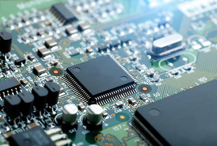
1. High Speed Signal Integrity Design
Logic devices often operate at high data rates. Proper PCB design includes:
-
Controlled impedance routing
-
Differential pair matching
-
Length matching for timing accuracy
-
Optimized stack-up design
These techniques minimize signal distortion and timing errors.
2. Stable Power Distribution Network (PDN)
Digital IC testing requires clean and stable power supply delivery. Logic Test PCBs feature:
-
Solid power and ground planes
-
Low impedance power routing
-
Decoupling capacitor optimization
-
Reduced voltage ripple and noise
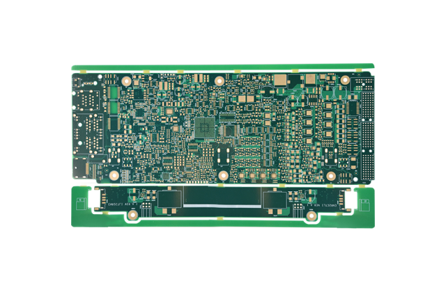
3. High Layer Count Capability
Complex logic devices may require:
-
Multi-layer routing
-
Dense BGA breakout
-
Fine pitch trace design
-
Microvia technology
High layer count PCBs help manage complex interconnections efficiently.
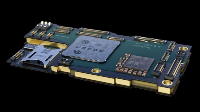
4. High Pin Count Support
Modern processors and FPGAs often feature hundreds or thousands of pins. Logic Test PCBs must support:
-
High-density interconnect (HDI) design
-
Fine line and fine pitch routing
-
Accurate pad and via positioning
Applications of Logic Test PCB
Logic Test PCBs are widely used in:
-
Semiconductor production testing
-
Functional verification platforms
-
Engineering validation test (EVT)
-
Design validation test (DVT)
-
Burn-in and reliability screening
-
ATE load boards for digital ICs
These boards play a key role in ensuring digital devices meet performance specifications before market release.
Design Considerations for Logic Test PCB
Signal Timing Accuracy
-
Length matching
-
Skew control
-
Clock routing optimization
Thermal Management
-
Heat spreading copper planes
-
Thermal vias
-
Stable mechanical structure
Mechanical Compatibility
-
Test socket integration
-
Stable fixture alignment
-
Repeated DUT insertion durability
Logic Test PCB vs RF Test PCB
| Feature | Logic Test PCB | RF Test PCB |
|---|---|---|
| Frequency Range | Digital high speed | RF / Microwave |
| Design Focus | Timing & Signal Integrity | Impedance & Loss Control |
| Materials | High TG FR-4 / Low loss | PTFE / RF laminates |
| Applications | MCU, FPGA, ASIC | RF IC, 5G, Radar |
Logic Test PCBs focus primarily on timing precision and digital signal integrity, while RF Test PCBs emphasize high-frequency performance.
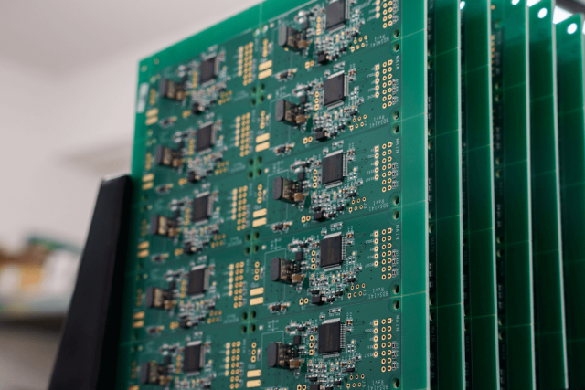
Choosing a Professional Logic Test PCB Manufacturer
A reliable Logic Test PCB supplier should provide:
-
High layer count fabrication
-
Fine pitch and HDI capability
-
Controlled impedance support
-
Stable mass production quality
-
Fast prototype turnaround
Partnering with an experienced semiconductor test PCB manufacturer ensures consistent test accuracy and long-term reliability.
Conclusion
Logic Test PCBs are essential for validating modern digital and logic devices. With precise impedance control, stable power distribution, and high-density routing capability, these boards enable accurate, repeatable semiconductor testing.
Selecting a professional Logic Test PCB manufacturer ensures improved yield, reduced false failures, and efficient production validation.
