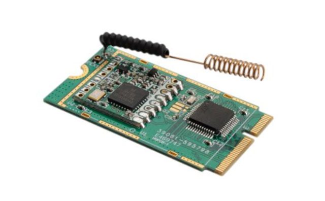
An IoT IC Test PCB is a specialized semiconductor test PCB designed to validate Internet of Things (IoT) integrated circuits, which often combine low-power analog, digital, and wireless communication functions in a compact package. These test PCBs are essential for reliable evaluation of power efficiency, signal integrity, and functional performance of IoT chips before deployment in connected devices.
By serving as the interface between IoT ICs and Automated Test Equipment (ATE), these PCBs ensure stable electrical connections, minimal noise, and repeatable test results across diverse IoT applications.
Key Design Considerations for IoT IC Test PCBs
1. Support for Low-Power and Mixed-Signal ICs
IoT ICs often operate at ultra-low voltages and contain both analog and digital domains. Test PCBs must minimize leakage, noise, and interference while maintaining reliable connectivity.
2. High Pin Count and HDI Routing
Compact IoT packages may still have high pin counts, requiring HDI technology, multilayer routing, fine-line traces, and microvias to ensure accurate testing and signal access.
3. Controlled Impedance and Signal Integrity
Wireless and high-speed interfaces demand precise controlled impedance routing, matched trace lengths, and proper grounding to avoid signal reflections and maintain measurement accuracy.
4. Robust Power Distribution
IoT IC test boards need an optimized power distribution network (PDN) with low-impedance planes and effective decoupling to ensure stable power during low-voltage, high-precision testing.
5. Mechanical Precision and Reliability
Accurate and repeatable probe or socket contact is critical. IoT IC test PCBs are designed with tight tolerances, flatness control, and reinforced structures to support repeated test cycles.
Applications of IoT IC Test PCBs
IoT IC test PCBs are widely used in:
-
Wireless communication module IC testing (BLE, Wi-Fi, Zigbee)
-
Sensor interface and analog front-end IC validation
-
Low-power MCU and logic IC qualification
-
Battery management and energy-harvesting IC testing
-
Industrial, consumer, and smart home IoT device validation
These applications require high measurement accuracy, low noise, and repeatable results to ensure IoT device reliability.
Manufacturing Requirements for IoT IC Test PCBs

High-quality IoT IC test PCBs require:
-
Multilayer and HDI PCB fabrication
-
Fine-line etching and microvia processing
-
Controlled impedance verification
-
Low-loss, low-leakage laminates suitable for low-power operation
-
Prototype, small batch, and volume production support
Strict process control ensures consistent electrical performance, high reliability, and precise testing for IoT semiconductor devices.
Why IoT IC Test PCB Quality Matters
Low-quality test boards can lead to:
-
Increased noise affecting analog or RF signals
-
Measurement errors or inconsistent test results
-
Lower test yield and extended debugging cycles
-
Potential failure in connected IoT devices
A professionally engineered IoT IC Test PCB ensures accurate validation, reliable performance, and efficient production testing for next-generation IoT devices.
Conclusion
The IoT IC Test PCB is essential for validating low-power, mixed-signal, and wireless integrated circuits used in IoT applications. With HDI routing, high pin count support, controlled impedance, and robust low-power design, these boards provide reliable, repeatable, and precise testing.
Partnering with an experienced IoT IC test PCB manufacturer ensures high test accuracy, faster validation cycles, and long-term reliability for IoT semiconductor devices.
