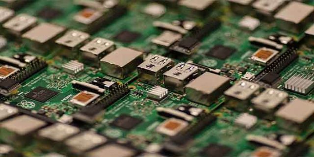
An IoT IC Test PCB is a specialized printed circuit board designed to validate low-power, high-density, and high-functionality IoT integrated circuits. These ICs combine analog, digital, RF, and sensor interfaces in compact packages, often operating at low voltages and requiring precise timing for wireless communication.
IoT IC test PCBs are widely used in Automated Test Equipment (ATE), load boards, and probe card systems to ensure accurate measurement, functional verification, and production reliability for IoT devices in smart homes, wearable electronics, industrial automation, and wireless sensors.
Key Design Considerations for IoT IC Test PCBs
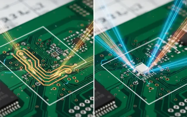
1. Low-Power Signal Integrity
IoT ICs often operate at sub-1V to 3.3V levels, making signal noise and voltage drops critical. IoT IC test PCBs require careful trace routing, low-loss materials, and controlled impedance to maintain accurate measurements.
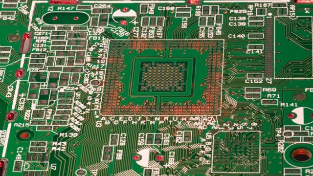
2. High-Density Component Layouts
Compact IoT IC packages demand multilayer PCB stackups, microvias, and via-in-pad technologies to support high pin counts without compromising signal quality.
3. RF and Wireless Testing
Many IoT ICs integrate Wi-Fi, Bluetooth, Zigbee, or LoRa transceivers. Test PCBs must provide low-loss RF routing, proper grounding, and isolation between analog, digital, and RF domains to ensure accurate high-frequency performance.
4. Thermal and Power Management
Even low-power ICs can generate localized hotspots during testing. IoT IC test PCBs often incorporate thermal vias, optimized copper planes, and multilayer power distribution networks to stabilize temperature and voltage during high-speed testing.
Structural Features of IoT IC Test PCBs
-
Controlled impedance traces for analog, digital, and RF signals
-
Compact multilayer stackups for high-density routing
-
Low-loss PCB materials for wireless signal integrity
-
Microvias, blind/buried vias, and via-in-pad designs for fine-pitch ICs
-
Optimized power distribution and thermal management
These features ensure accurate, repeatable, and reliable testing of IoT ICs in both prototype and production environments.
Applications of IoT IC Test PCBs
IoT IC test PCBs are used in:
-
Smart home and wearable device IC testing
-
Wireless sensor network IC validation
-
Low-power microcontroller and SoC testing
-
Industrial IoT and automation IC characterization
-
Load boards and probe cards for ATE systems
Reliable test PCBs are critical for maintaining signal integrity, low noise, and accurate functional testing in IoT applications.
Manufacturing Requirements for IoT IC Test PCBs
Producing high-quality IoT IC test PCBs requires:
-
Precise impedance and trace control
-
Advanced multilayer lamination and via processing
-
Low-loss PCB materials for RF and analog signals
-
Electrical verification for signal integrity and repeatability
-
Support for prototype, small batch, and mass production
A professional manufacturer ensures consistent quality, fast turnaround, and high reliability in semiconductor testing environments.
Conclusion
An IoT IC Test PCB is essential for accurate validation of connected, low-power integrated circuits. Through controlled impedance routing, multilayer construction, microvia technology, and optimized thermal management, these PCBs deliver highly reliable, repeatable, and precise IC testing.
Partnering with an experienced IoT IC test PCB manufacturer ensures consistent test results, efficient production support, and robust validation for IoT devices from development to mass production.
