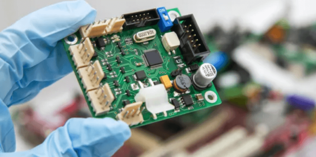
An IoT IC Test PCB is a specialized semiconductor test board designed to validate Internet-of-Things (IoT) integrated circuits, including sensors, microcontrollers, RF transceivers, and mixed-signal ICs. Installed in Automated Test Equipment (ATE) systems, these test PCBs ensure precise signal transmission, reliable power delivery, and accurate measurement of IoT devices during both R&D validation and production testing.
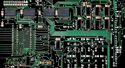
IoT ICs often combine low-power digital circuits, RF communication, and analog sensors, requiring a highly reliable, low-noise, and controlled test environment. Standard IC test boards cannot guarantee the accuracy needed for modern IoT semiconductor validation.
Key Design Requirements of IoT IC Test PCBs

1. Controlled Impedance and Signal Integrity
IoT ICs often use high-speed digital and RF communication interfaces such as BLE, Zigbee, Wi-Fi, or LoRa. Controlled impedance traces and optimized stackups ensure minimal signal reflection and stable high-frequency performance.
2. Low-Loss Materials and High-Frequency Routing
To maintain signal fidelity, low-loss laminates are used for RF paths, and HDI PCB technology enables dense fan-out routing for fine-pitch IoT IC packages.
3. Power Integrity and Noise Isolation
IoT ICs are sensitive to power fluctuations and noise. Proper power plane design, decoupling, and grounding techniques minimize voltage ripple and interference, ensuring accurate test results.
4. High-Density Routing and Compact Design
Modern IoT IC packages feature high I/O counts in small footprints. High-density HDI routing ensures that even complex IoT devices are tested reliably.
5. Mechanical Stability and Test Socket Alignment
Accurate alignment with test sockets is essential for consistent electrical contact during repeated insertion cycles, particularly for sensor and MEMS ICs.
Applications of IoT IC Test PCBs
IoT IC test PCBs are widely used for testing:
-
Sensor ICs and MEMS devices
-
Low-power microcontrollers and SoCs
-
IoT RF transceivers (BLE, Zigbee, Wi-Fi, LoRa)
-
Mixed-signal IoT devices
-
Smart home, industrial, automotive, and wearable IoT electronics
These applications demand high-precision, low-noise, and repeatable test results.
Manufacturing Capabilities for IoT IC Test PCBs
Reliable IoT IC test PCBs require advanced manufacturing expertise:
-
Controlled impedance and low-loss RF routing
-
Multilayer and HDI PCB fabrication
-
Precision drilling and fine-line etching
-
Prototype, small batch, and volume production support
-
High-Tg and low-Dk laminates for IoT RF signals
Such capabilities ensure consistent performance for IoT IC validation from early prototyping to mass production.
Why IoT IC Test PCB Quality Matters

A poorly designed IoT IC test PCB can cause signal degradation, measurement errors, and reduced yield. A high-quality test board ensures:
-
Accurate RF and digital measurements
-
Minimal noise interference and crosstalk
-
Reliable testing during repeated insertion cycles
-
Improved throughput and semiconductor testing efficiency
Conclusion
The IoT IC Test PCB is a critical element in IoT semiconductor testing, enabling precise validation of high-speed, low-power, and mixed-signal devices. With controlled impedance, low-loss materials, HDI routing, and robust power integrity, IoT IC test PCBs ensure reliable, repeatable, and accurate testing results.
Partnering with an experienced IoT IC test PCB manufacturer guarantees consistent quality, faster time-to-market, and long-term reliability for IoT device production.
