What is a High Layer Count PCB?
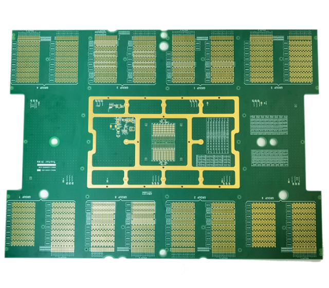
A High Layer Count PCB refers to a multilayer printed circuit board with a large number of layers, typically 10 layers and above, and often reaching 20, 30, or even 50+ layers in advanced applications.
A high layer count PCB is designed to handle complex routing, high-speed signals, and dense component layouts, making it essential for modern high-performance electronic systems.
Why High Layer Count PCB is Needed
As electronic systems become more complex, standard multilayer PCBs are no longer sufficient. A high layer count PCB enables:
- Increased routing capacity
- Better signal isolation
- Improved power distribution
- Enhanced signal integrity
Typical Layer Count Ranges
| PCB Type | Layer Count |
|---|---|
| Standard PCB | 2–8 layers |
| Multilayer PCB | 8–16 layers |
| High Layer Count PCB | 16–50+ layers |
Key Features of High Layer Count PCB
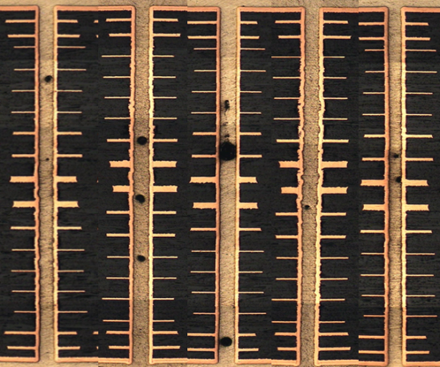
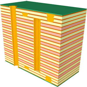
1. Complex Stack-Up Design
High layer count PCB requires carefully planned stack-up to manage signal integrity and power distribution.
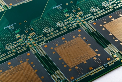
2. High Routing Density
Supports complex circuits with high pin-count components.
3. Controlled Impedance
Essential for high-speed and RF applications.
4. Signal Isolation
Multiple layers help reduce noise and crosstalk.
High Layer Count PCB vs Standard Multilayer PCB
| Feature | High Layer Count PCB | Standard PCB |
|---|---|---|
| Complexity | Very High | Moderate |
| Routing Density | High | Medium |
| Layer Count | 16+ | <16 |
| Manufacturing Difficulty | High | Lower |
Applications of High Layer Count PCB
1. Networking & Data Centers
Routers, switches, and high-speed communication systems.
2. Aerospace & Defense
Radar, avionics, and mission-critical systems.
3. Medical Equipment
High-precision diagnostic systems.
4. Industrial Systems
Complex control and automation systems.
5. High-Performance Computing
Servers and AI hardware platforms.
Design Considerations
1. Stack-Up Optimization
Layer arrangement must balance signal, power, and ground planes.
2. Signal Integrity Management
High-speed signals require impedance control and isolation.
3. Thermal Management
More layers can trap heat, requiring careful design.
4. Power Distribution
Stable power planes are critical in high layer count PCB.
Manufacturing Challenges
Producing a high layer count PCB is highly demanding:
1. Lamination Cycles
Multiple lamination steps increase process complexity.
2. Layer Alignment
Precise registration is critical across all layers.
3. Drill Accuracy
Deep drilling requires high precision to avoid misalignment.
4. Yield Control
Higher layer count increases defect risk.
Material Considerations
High layer count PCB often uses:
- High Tg FR4 for stability
- Low loss materials for high-speed designs
- Specialized laminates for RF applications
When Should You Use High Layer Count PCB?
Choose high layer count PCB when:
- Circuit complexity is very high
- High-speed signals require isolation
- High pin-count components are used
- System integration level is high
Avoid it when:
- Design is simple
- Cost is the main constraint
- Lower layer count can meet requirements
Conclusion
High Layer Count PCB technology enables complex, high-performance electronic systems by providing the routing density, signal integrity, and scalability required in advanced designs.
Successful implementation depends on proper design, material selection, and manufacturing expertise.
