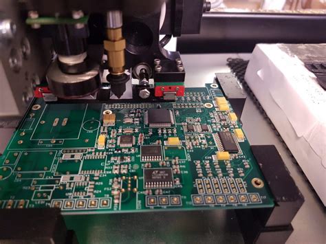
As automated test equipment evolves to support faster data rates and higher pin counts, PCB complexity increases significantly. The High Layer Count ATE PCB provides the routing density, power integrity, and signal control required for modern semiconductor testing.
High layer count designs are essential for advanced ATE performance and scalability.
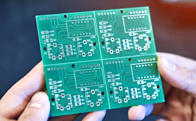
What Is a High Layer Count ATE PCB?
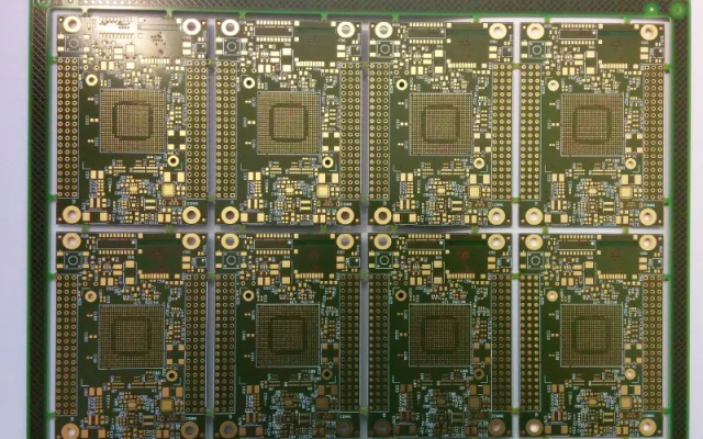
A High Layer Count ATE PCB typically features 16 layers or more, combining multiple signal, power, and ground planes within a compact footprint. These boards are engineered to support complex test architectures and high-density device interfaces.
Why High Layer Count Is Critical in ATE Systems
High layer count ATE PCBs allow engineers to:
-
Route thousands of high-speed signals
-
Isolate sensitive analog and digital domains
-
Distribute power efficiently across the board
Layer count directly impacts test accuracy and system stability.
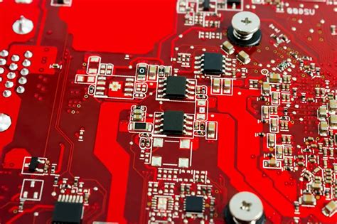
Signal Integrity in High Layer Count Designs
Maintaining clean signals across many layers requires:
-
Controlled impedance routing
-
Consistent dielectric thickness
-
Proper reference plane pairing
These measures minimize crosstalk and signal loss.
Power Integrity and Ground Management
High pin count devices demand stable power. High layer count ATE PCBs incorporate:
-
Dedicated power planes for each voltage domain
-
Low-inductance ground structures
-
Extensive decoupling strategies
This ensures reliable operation during high-speed testing.
Stackup Planning and Material Selection
Stackup design is critical in high layer count ATE PCBs. Engineers consider:
-
Symmetrical layer construction
-
Low-loss dielectric materials
-
Thermal stability and CTE matching
Proper stackup reduces warpage and improves yield.
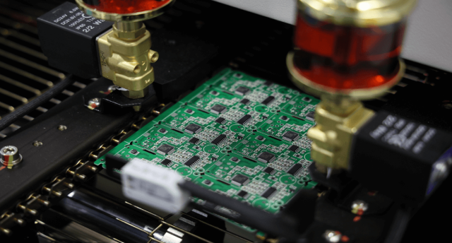
Manufacturing Challenges and Process Control
Producing high layer count ATE PCBs requires:
-
Precise layer alignment
-
Advanced lamination techniques
-
Strict quality and electrical testing
Manufacturing expertise is essential for consistent performance.
Applications of High Layer Count ATE PCBs
These PCBs are commonly used in:
-
Semiconductor device testing
-
High-speed digital and mixed-signal ATE
-
Advanced probe and load board systems
-
Next-generation test platforms
High layer count designs enable scalability and flexibility.
Choosing a High Layer Count ATE PCB Manufacturer
When selecting a high layer count ATE PCB supplier, look for:
-
Proven multilayer manufacturing capability
-
Experience with test and semiconductor boards
-
Controlled impedance and SI/PI expertise
-
Engineering support from prototype to production
A qualified partner reduces risk and accelerates development.
Conclusion
The High Layer Count ATE PCB is a foundational element in advanced automated test equipment. By enabling dense routing, stable power delivery, and controlled signal behavior, high layer count ATE PCBs support accurate, repeatable, and scalable semiconductor testing.
Partnering with an experienced high layer count ATE PCB manufacturer ensures reliable performance from engineering validation to mass production.
