As RF, microwave, and high-speed digital technologies continue to advance, test environments must deliver exceptional signal fidelity. The High Frequency Test PCB is specifically designed to support precise signal transmission, minimal loss, and repeatable measurement results at high frequencies.
A properly engineered high frequency test PCB is essential for reliable RF and high-speed validation.
What Is a High Frequency Test PCB?
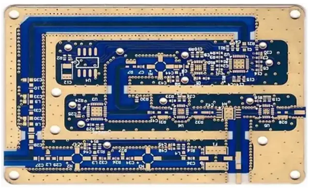
A High Frequency Test PCB is a printed circuit board optimized for testing signals operating from hundreds of MHz to millimeter-wave frequencies. Unlike standard test boards, it prioritizes signal integrity and measurement accuracy over general-purpose functionality.
Why High Frequency Test PCBs Are Critical
High frequency test PCBs are essential because they:
-
Minimize insertion loss and signal distortion
-
Preserve waveform integrity during testing
-
Ensure consistent and repeatable test results
These requirements are critical for RF and high-speed validation.
Controlled Impedance and Transmission Line Design
Accurate impedance control is fundamental. High frequency test PCBs incorporate:
-
Precisely calculated trace geometries
-
Consistent dielectric thickness
-
Continuous reference planes
These factors ensure stable impedance across the board.
Low-Loss Materials for High Frequency Testing
Material selection directly impacts test accuracy. High frequency test PCBs commonly use:
-
Rogers and PTFE-based laminates
-
Low-loss FR-4 variants for mixed designs
-
Hybrid stackups for cost and performance balance
Low dielectric loss reduces signal attenuation.
Stackup Optimization for RF Test Performance
Optimized stackups are designed to:
-
Shorten signal paths
-
Reduce parasitic effects
-
Improve electromagnetic field control
Careful stackup planning enhances measurement reliability.
Via Design and RF Transitions
Vias can degrade high frequency signals if poorly designed. High frequency test PCBs use:
-
Back-drilled vias to remove stubs
-
Short via transitions
-
Optimized via-to-plane clearances
These techniques minimize reflection and loss.
EMI and Crosstalk Control
High frequency testing environments require:
-
Proper spacing between RF channels
-
Ground stitching vias
-
Shielding structures where necessary
Effective EMI control improves test repeatability.
Manufacturing Precision and Verification
Manufacturing high frequency test PCBs demands:
-
Tight impedance tolerances
-
Controlled dielectric consistency
-
Electrical and impedance testing
Strict process control ensures accurate results.
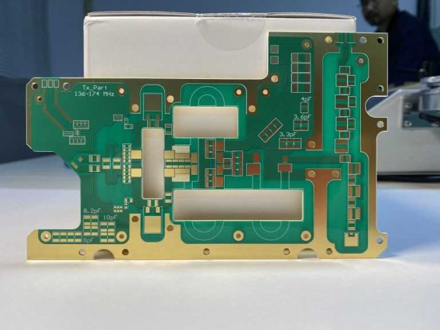
Typical Applications of High Frequency Test PCBs
High frequency test PCBs are widely used in:
-
RF and microwave device testing
-
Semiconductor validation and characterization
-
5G and mmWave test platforms
-
High-speed communication system testing
These applications rely on precise signal measurement.
Selecting a High Frequency Test PCB Manufacturer
When choosing a high frequency test PCB supplier, consider:
-
Experience with RF and microwave materials
-
Controlled impedance and RF testing capability
-
Support for prototype and small-batch production
-
Engineering collaboration during design review
An experienced partner ensures accurate and reliable test boards.
Conclusion
The High Frequency Test PCB plays a crucial role in ensuring accurate RF and high-speed signal testing. Through low-loss materials, controlled impedance routing, and precision manufacturing, these PCBs deliver stable and repeatable test performance.
Working with a specialized high frequency test PCB manufacturer helps achieve reliable results in demanding test environments.
