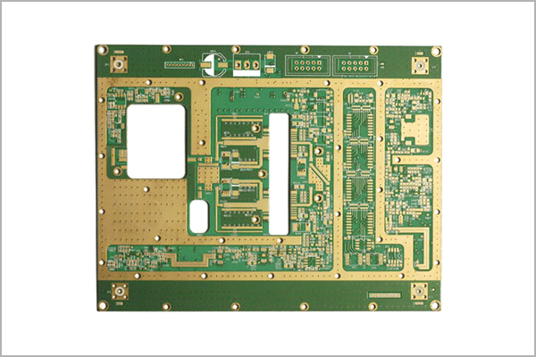
In RF, microwave, and high-speed electronic testing, even minor PCB imperfections can introduce significant measurement errors. The High Frequency Test PCB is engineered to serve as a neutral and stable signal platform, allowing engineers to evaluate devices and systems with confidence.
A properly designed high frequency test PCB ensures that test results reflect device performance—not PCB-induced distortion.
The Role of High Frequency Test PCBs in Validation
High frequency test PCBs are not functional products but precision measurement tools. Their primary purpose is to:
-
Preserve original signal characteristics
-
Eliminate unnecessary loss and reflection
-
Maintain consistency across repeated tests
This makes them critical in RF and high-speed validation environments.
Frequency Range and Design Considerations
High frequency test PCBs typically operate from:
-
Several hundred MHz
-
Multiple GHz
-
Up to mmWave frequencies
As frequency increases, PCB geometry, materials, and transitions become dominant factors in signal behavior.
Controlled Impedance as a Test Foundation
Impedance deviations directly affect test accuracy. High frequency test PCBs rely on:
-
Precisely calculated transmission line structures
-
Tight dielectric thickness control
-
Stable reference planes
Consistent impedance ensures accurate S-parameter and time-domain measurements.
Low-Loss Dielectrics and Surface Roughness Control
Material and copper quality significantly impact signal loss. High frequency test PCBs often use:
-
Low-Dk, low-Df laminates
-
Smooth copper foil for reduced conductor loss
-
Hybrid stackups for cost-sensitive designs
These choices minimize attenuation and phase distortion.
Via Transitions and RF Interconnect Optimization
Poorly designed vias introduce reflections and resonance. High frequency test PCBs implement:
-
Short via stubs or back-drilling
-
Grounded via fences near signal vias
-
Optimized launch structures
Clean transitions improve bandwidth and measurement repeatability.
Crosstalk and EMI Suppression
In dense test setups, unwanted coupling degrades accuracy. Effective solutions include:
-
Adequate signal spacing
-
Ground stitching vias
-
Shielded routing zones
Proper isolation ensures clean test data.
Stackup Symmetry and Mechanical Stability
Test PCBs must remain stable over time and temperature. Stackups are designed to:
-
Minimize warpage
-
Maintain consistent dielectric properties
-
Support precise connector alignment
Mechanical stability directly impacts test consistency.
Manufacturing Accuracy and Validation
Producing high frequency test PCBs requires:
-
Tight process tolerances
-
Impedance coupon testing
-
Electrical and visual inspection
Manufacturing precision ensures that test boards perform as designed.
Typical Applications of High Frequency Test PCBs
High frequency test PCBs are widely used in:
-
RF and microwave component validation
-
5G and mmWave module testing
-
Semiconductor characterization
-
High-speed interface compliance testing
Each application demands predictable signal behavior.
Selecting a High Frequency Test PCB Manufacturer
When choosing a high frequency test PCB supplier, engineers should consider:
-
Experience with RF and microwave PCB fabrication
-
Controlled impedance and low-loss material capability
-
Support for prototype and engineering builds
-
Understanding of test-driven design priorities
The right partner helps ensure measurement integrity.
Conclusion
The High Frequency Test PCB plays a crucial role in accurate RF and microwave validation. By minimizing loss, reflection, and noise, it allows engineers to trust their test results and make informed design decisions.
Collaborating with an experienced high frequency test PCB manufacturer ensures reliable, repeatable, and high-precision test performance.
