As RF, microwave, and high-speed electronic systems continue to evolve, product complexity and performance requirements are increasing rapidly. High frequency PCB ODM services provide a complete solution by combining design expertise with advanced manufacturing, enabling customers to accelerate development while ensuring stable RF performance.
A professional high frequency PCB ODM partner bridges the gap between concept, engineering, and mass production.
What Is High Frequency PCB ODM?
High frequency PCB ODM (Original Design Manufacturing) refers to a service model where the manufacturer supports both PCB design and fabrication, specifically for high-frequency and high-speed applications.
Unlike standard PCB fabrication, a high frequency PCB ODM partner:
-
Participates in RF and high-speed design decisions
-
Recommends suitable low-loss materials
-
Optimizes stackups for impedance and signal integrity
-
Manufactures and tests PCBs under one integrated system
This approach reduces design risk and improves overall product performance.
Why Choose High Frequency PCB ODM Services?
Design for RF Performance
High-frequency circuits are highly sensitive to layout, impedance, and material selection. An experienced high frequency PCB ODM team provides:
-
RF layout optimization
-
Impedance calculation and simulation
-
Stackup and grounding strategy design
This ensures signal integrity from the earliest design stage.
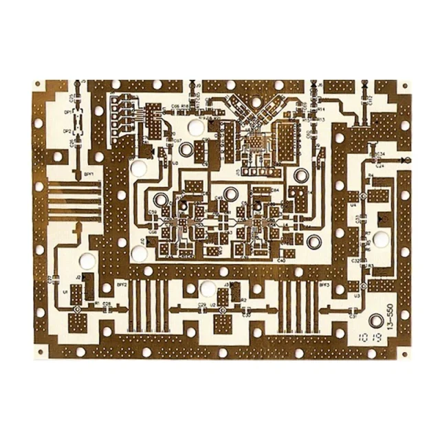
Material Expertise for High Frequency Applications
A reliable high frequency PCB ODM supports a wide range of RF materials, including:
-
Rogers series laminates
-
PTFE and Duroid materials
-
Low-loss hybrid stackups
-
High-Tg FR-4 for mixed-signal designs
Correct material selection directly impacts insertion loss, phase stability, and thermal reliability.
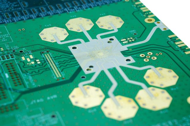
Controlled Impedance and Signal Integrity
High frequency PCB ODM manufacturing emphasizes precise impedance control:
-
Tight tolerance control on dielectric thickness
-
Accurate copper geometry management
-
Controlled impedance fabrication (±5% or better)
-
TDR testing and validation
These processes minimize signal reflection and ensure consistent RF performance.
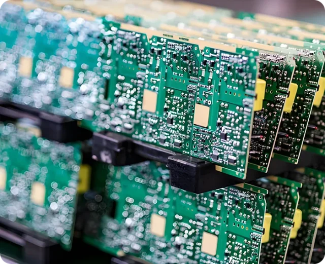
Manufacturing Integration Advantages
By combining design and fabrication, high frequency PCB ODM services deliver:
-
Faster design iterations
-
Fewer engineering change orders (ECOs)
-
Higher first-pass yield
-
Smoother transition from prototype to mass production
Integrated workflows improve efficiency and product reliability.
Applications of High Frequency PCB ODM
High frequency PCB ODM services are widely used in:
-
RF front-end modules
-
5G and mmWave communication systems
-
Automotive radar and ADAS electronics
-
High-speed data transmission hardware
-
Industrial RF and sensing systems
-
Advanced IoT and wireless devices
These applications require stable high-frequency performance and repeatable manufacturing quality.
Prototype to Mass Production Support
A qualified high frequency PCB ODM partner supports the full product lifecycle:
-
Small-batch PCB prototypes
-
Engineering validation builds
-
Pilot runs and DFM optimization
-
Scalable mass production
This continuity ensures consistent electrical performance across all production stages.
Choosing the Right High Frequency PCB ODM Partner
When selecting a high frequency PCB ODM, evaluate:
-
RF and high-speed design experience
-
Material and stackup expertise
-
Controlled impedance and RF testing capability
-
Proven manufacturing quality systems
-
Clear communication between design and production teams
A strong ODM partner functions as an extension of your engineering team.
Conclusion
High frequency PCB ODM services provide a powerful solution for companies developing RF and high-speed electronic products. By integrating design expertise, material knowledge, and precision manufacturing, an experienced ODM partner reduces development risk, shortens time to market, and ensures stable high-frequency performance.
Choosing the right high frequency PCB ODM partner is a strategic decision that directly impacts product reliability and long-term success.
