As IoT devices increasingly rely on wireless communication, RF and high-frequency circuit performance becomes critical from the earliest design stage. A high frequency IoT PCB prototype allows engineers to validate RF performance, antenna behavior, and high-speed signal integrity before moving into mass production.
Reliable high frequency IoT PCB prototyping reduces development risk, shortens time to market, and improves overall product performance.
What Is a High Frequency IoT PCB Prototype?
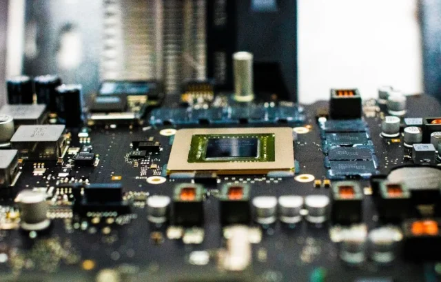
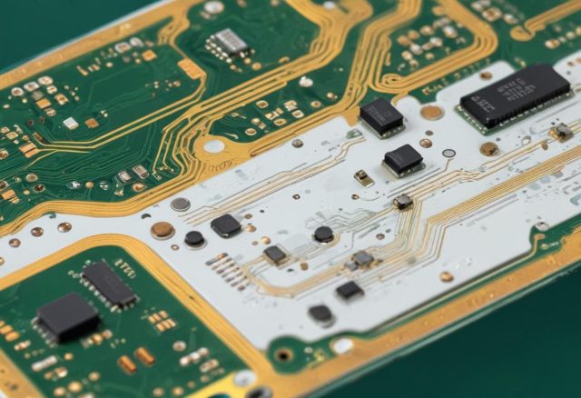
A high frequency IoT PCB prototype is an early-stage PCB built using RF or high-frequency materials to support wireless communication standards such as LTE, 5G, Wi-Fi, Bluetooth, LoRa, and NB-IoT.
These prototypes often include:
-
RF transceivers and antennas
-
High-speed digital interfaces
-
Controlled impedance traces
-
Compact and high-density layouts
Why High Frequency PCB Prototypes Are Critical for IoT Devices
Early RF Performance Validation
Prototyping helps verify antenna tuning, impedance matching, and RF signal loss under real operating conditions.
Signal Integrity Testing
High frequency IoT PCB prototypes allow engineers to evaluate crosstalk, insertion loss, and EMI performance before finalizing designs.
Fast Design Iteration
Rapid prototype cycles enable quick design updates and performance optimization.
Materials Used for High Frequency IoT PCB Prototypes
Professional high frequency IoT PCB prototype services support advanced materials such as:
-
Rogers RO4003 / RO4350
-
Taconic RF series
-
PTFE-based laminates
-
Hybrid RF + FR-4 stackups
Material selection directly affects RF stability and cost efficiency.
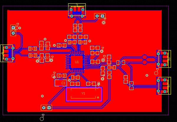
Controlled Impedance in High Frequency IoT PCB Prototypes
Accurate impedance control is essential in high frequency IoT PCB prototype manufacturing. This includes:
-
Stackup simulation and impedance calculation
-
Tight tolerance control during fabrication
-
Controlled impedance production (±5% or tighter)
-
TDR impedance testing and reporting
Rapid Turnaround for IoT PCB Prototyping
A professional high frequency IoT PCB prototype manufacturer offers:
-
Quick-turn fabrication services
-
Small batch prototype production
-
Engineering feedback and DFM support
-
Seamless transition to mass production
Fast turnaround accelerates IoT product development.
Testing and Validation for IoT PCB Prototypes
Testing is a critical part of high frequency IoT PCB prototype development, including:
-
Electrical continuity testing
-
Impedance verification
-
RF performance testing
-
Functional validation at the module level
Comprehensive testing ensures prototype reliability.
Applications of High Frequency IoT PCB Prototypes
High frequency IoT PCB prototypes are widely used in:
-
Wireless IoT modules
-
Smart sensors and gateways
-
Industrial IoT devices
-
Wearable and smart home products
-
Asset tracking and monitoring systems
These applications demand stable RF performance and compact design.
Choosing a Partner for High Frequency IoT PCB Prototyping
When selecting a supplier for high frequency IoT PCB prototype, consider:
-
Experience with RF and IoT PCB designs
-
Controlled impedance and RF testing capability
-
Fast prototype turnaround
-
Engineering support and scalability
The right partner reduces development risk and speeds up product validation.
Conclusion
High frequency IoT PCB prototype development is essential for validating RF performance and signal integrity in modern wireless IoT devices. With the right materials, controlled impedance, and rapid prototyping support, manufacturers can accelerate product validation and ensure successful mass production.
Partnering with an experienced PCB manufacturer ensures reliable, high-performance high frequency IoT PCB prototypes from concept to production.
