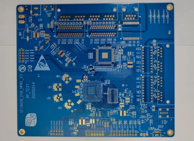
As IoT devices increasingly rely on high-speed wireless communication, the demand for high frequency IoT PCB prototypes has grown rapidly. From Wi-Fi, Bluetooth, LTE, and NB-IoT to emerging 5G IoT applications, early-stage PCB prototypes play a critical role in validating RF performance, signal integrity, and system reliability.
A well-designed high frequency IoT PCB prototype allows engineers to identify performance risks early and accelerate product development.
Why High Frequency Matters in IoT PCB Prototyping
Modern IoT devices often integrate:
-
High-frequency RF transceivers
-
Compact antennas and RF front-end modules
-
High-speed digital interfaces
At higher frequencies, even minor PCB design or material issues can significantly impact wireless range, power consumption, and communication stability. This makes high frequency IoT PCB prototyping essential for performance validation.
Key Objectives of a High Frequency IoT PCB Prototype
A professional high frequency IoT PCB prototype focuses on:
-
Verifying RF signal integrity and impedance matching
-
Evaluating antenna performance and radiation efficiency
-
Measuring insertion loss and noise levels
-
Confirming layout, stackup, and grounding strategies
Prototype testing ensures the design meets real-world operating conditions before scaling to production.
Material Selection for High Frequency IoT PCB Prototypes
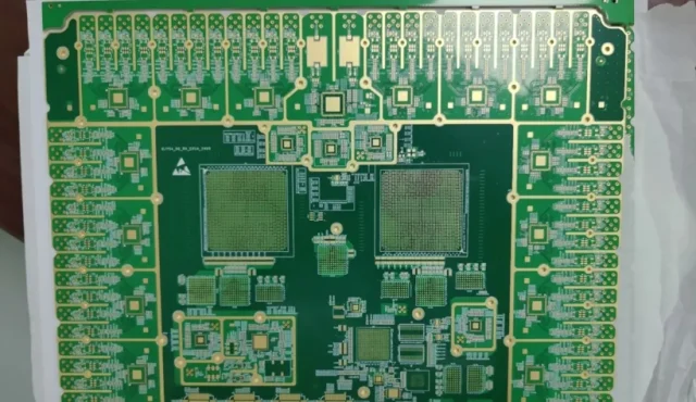
Material choice directly impacts RF performance. Common materials used in high frequency IoT PCB prototypes include:
-
Low-loss FR-4 for cost-sensitive IoT devices
-
Rogers RO4003 / RO4350 for stable RF performance
-
Hybrid stackups combining RF laminates and FR-4
Selecting the right material balances cost, performance, and manufacturability during the prototype stage.
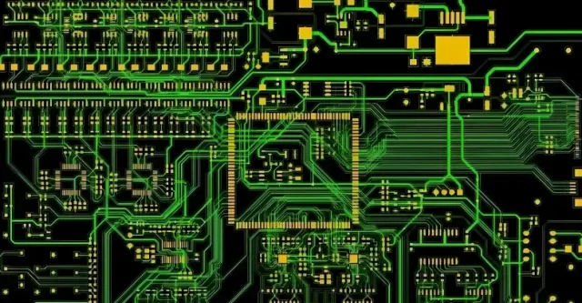
Controlled Impedance in IoT RF PCB Prototypes
Wireless IoT designs rely on precise impedance control. A qualified manufacturer ensures:
-
Controlled impedance transmission lines
-
Consistent dielectric thickness and trace geometry
-
TDR impedance verification during prototyping
Proper impedance control reduces signal reflection and improves communication reliability.
Rapid Iteration and Design Validation
One of the biggest advantages of a high frequency IoT PCB prototype is fast iteration:
-
Quick turnaround prototype fabrication
-
Small batch builds for RF tuning
-
Design feedback and layout optimization
Rapid prototyping allows engineers to refine antenna placement, RF routing, and power integrity before mass production.
Manufacturing Considerations for High Frequency IoT PCB Prototypes
Producing reliable IoT RF prototypes requires:
-
Fine-line etching for compact RF layouts
-
Controlled copper surface roughness
-
Stable lamination for multilayer boards
-
Electrical and impedance testing
These processes ensure prototype results accurately represent production performance.
Typical Applications of High Frequency IoT PCB Prototypes
High frequency IoT PCB prototypes are widely used in:
-
Smart home and smart city devices
-
Industrial IoT sensors and gateways
-
Wearable and portable wireless devices
-
Asset tracking and positioning systems
-
Low-power wide-area network (LPWAN) devices
Each application benefits from early RF validation.
From High Frequency IoT PCB Prototype to Mass Production

A successful prototype should seamlessly transition to production. Working with an experienced manufacturer ensures:
-
Consistent materials and stackups
-
Scalable manufacturing processes
-
Stable RF performance in volume
This continuity reduces risk and shortens time-to-market.
Conclusion
A high frequency IoT PCB prototype is a critical step in developing reliable wireless IoT products. By validating RF performance, impedance control, and material behavior early, engineers can optimize designs, reduce development risk, and accelerate commercialization.
Partnering with a manufacturer experienced in high frequency IoT PCB prototyping ensures accurate results, faster iteration, and a smooth transition from concept to mass production.
