Fine Line PCB: High-Density Circuit Design for Advanced Electronics
As electronic devices continue to become smaller, faster, and more integrated, traditional PCB manufacturing technologies are often insufficient to meet the demands of modern circuit density. Fine Line PCB technology enables the creation of extremely narrow traces and spaces, allowing engineers to design highly compact and complex circuit boards for advanced electronic systems.
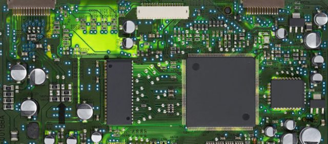
Fine line PCB fabrication plays a critical role in industries such as consumer electronics, telecommunications, medical devices, and high-performance computing, where miniaturization and high-density interconnection are essential.
What Is a Fine Line PCB?
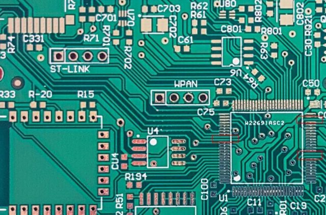
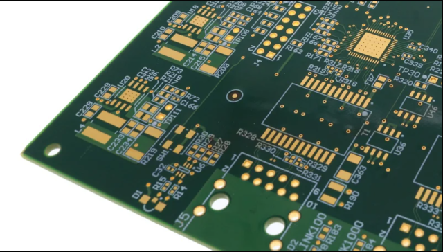
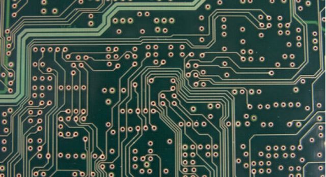
A Fine Line PCB refers to a printed circuit board manufactured with very narrow trace widths and spacing. Typically, fine line PCB designs feature line widths and spacing of 3 mil (75 µm) or smaller, enabling higher circuit density compared to conventional PCB layouts.
Advanced manufacturing techniques allow even finer structures, sometimes reaching 2 mil, 1.5 mil, or smaller, depending on the PCB technology and materials used.
Fine line PCBs are commonly used in:
-
High-density multilayer PCBs
-
HDI (High-Density Interconnect) circuit boards
-
Miniaturized consumer electronics
-
Advanced communication devices
Advantages of Fine Line PCB Technology
1. Higher Circuit Density
Fine line PCB designs enable more routing channels within the same board area, supporting compact product designs and complex circuitry.
2. Miniaturization of Electronic Devices
As devices become smaller and thinner, fine line PCB technology allows engineers to reduce PCB size while maintaining functionality.
3. Improved Signal Routing Flexibility
With smaller traces and tighter spacing, designers can route high-speed signals more efficiently in multilayer PCB layouts.
4. Compatibility with HDI PCB Technology
Fine line PCBs are often used together with HDI PCB technologies such as microvias, blind vias, and buried vias to achieve ultra-high interconnect density.
Fine Line PCB Manufacturing Techniques
Producing fine line PCBs requires advanced fabrication processes and precise manufacturing control. Key technologies include:
-
Laser Direct Imaging (LDI) for accurate circuit patterning
-
Advanced etching processes to achieve precise trace geometries
-
High-resolution photoresist materials
-
Microvia drilling technology for HDI boards
These processes help maintain tight tolerances required for fine line PCB structures.
Design Considerations for Fine Line PCB
Designing a reliable fine line PCB requires attention to several important factors:
-
Trace width and spacing tolerance
-
Copper thickness selection
-
Controlled impedance routing for high-speed signals
-
Signal integrity and crosstalk prevention
-
Manufacturability constraints
Close collaboration between designers and PCB manufacturers ensures that the fine line PCB layout meets both electrical performance and production requirements.
Applications of Fine Line PCB
Fine line PCB technology is widely used in modern electronics, including:
-
Smartphones and wearable devices
-
High-speed networking equipment
-
Medical electronics
-
Automotive electronics
-
Industrial control systems
-
High-performance computing hardware
In these applications, fine line PCBs enable compact designs without compromising performance or reliability.
Challenges in Fine Line PCB Manufacturing
Although fine line PCBs provide significant advantages, they also present manufacturing challenges:
-
Higher fabrication complexity
-
Tighter process control requirements
-
Increased sensitivity to etching variations
-
Greater inspection and quality control demands
Advanced PCB manufacturers use specialized equipment and strict process control to ensure consistent fine line PCB quality.
Conclusion
Fine Line PCB technology is essential for modern high-density electronic design. By enabling ultra-narrow trace widths and tight spacing, fine line PCBs support compact device architectures and advanced circuit complexity.
As electronic products continue to evolve toward higher integration and miniaturization, fine line PCB manufacturing will remain a key technology in next-generation electronic systems.
