1. Engineering Overview / Abstract
As precision RF test and measurement systems extend into the 40 – 110 GHz range, achieving sub-degree phase accuracy and minimal insertion-loss drift becomes a primary design requirement.
Taconic RF-35 PCBs—engineered with a glass-reinforced PTFE composite (Dk = 3.50 ± 0.05, Df = 0.0018 @ 10 GHz)—enable calibration-grade impedance consistency and low-loss performance across temperature cycles.
KKPCB integrates advanced lamination control and inline RF verification to ensure that the theoretical dielectric uniformity of RF-35 translates directly into real-world metrology stability.
2. Engineering Context & Technical Challenges
In precision VNA calibration modules, power-sensor backplanes, and mmWave fixtures built on Taconic RF-35 PCB substrates, even slight dielectric fluctuation or copper-roughness variation can distort S-parameters and cause calibration drift.
| Design Challenge | Root Cause | Engineering Impact |
|---|---|---|
| Phase instability | Dk variation vs temperature | Calibration reference error |
| Insertion-loss variation | Copper roughness and etch tolerance | Amplitude imbalance |
| Impedance mismatch | Lamination skew or resin-rich zones | Return-loss degradation |
| Connector fatigue | Repetitive coupling cycles | Microcrack formation → impedance shift |
These issues directly affect repeatability and traceability of RF test results, where the Taconic RF-35 PCB’s dielectric stability is fundamental to ensuring calibration integrity.
3. Material Science and Performance Characteristics
Taconic RF-35 offers an excellent trade-off between mechanical strength and RF loss performance.
-
Dk = 3.50 ± 0.05, Df = 0.0018 @ 10 GHz
-
CTE (Z-axis): ~ 35 ppm/°C, ensuring copper-PTFE alignment
-
Thermal Conductivity: 0.25 W/m·K
Compared with FR-4 (Df ≈ 0.018), RF-35 exhibits nearly 90 % lower loss tangent, enabling more stable insertion-loss response up to 110 GHz.
This makes it ideal for calibration standards and high-linearity mmWave reference boards.
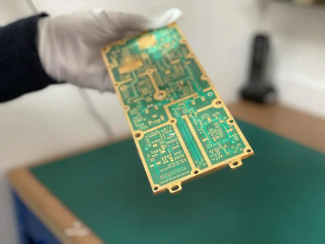
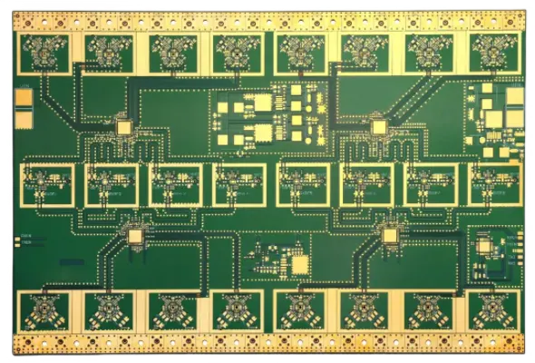
4. KKPCB Engineering Case Study — VNA Calibration Module
Client & Application
Japanese RF instrumentation manufacturer seeking sub-1° phase stability for VNA calibration fixtures.
Engineering Problem
Legacy PTFE boards showed 1.8° phase drift after 500 thermal cycles, exceeding calibration tolerance.
-
Implemented vacuum lamination with controlled resin flow (± 8 µm thickness tolerance)
-
Applied ½ oz rolled copper (Ra < 0.8 µm) for low surface loss
-
Integrated inline VNA verification per panel (10 – 110 GHz)
| Parameter | Target | KKPCB Result |
|---|---|---|
| Phase Deviation | < 1° @ 50 GHz | 0.78° |
| Insertion Loss | < 0.30 dB/in | 0.27 dB/in |
| Return Loss | > 15 dB | 16.8 dB |
| Connector Endurance | 1000 cycles | Pass (no impedance shift) |
Outcome: Phase drift reduced by 56 % vs legacy boards, ensuring calibration repeatability across production lots.
5. Stackup Design & RF Implementation
KKPCB employed a 4-layer hybrid RF-35 + FR-408 core with balanced CTE stackup.
-
Controlled copper roughness (Ra < 1.0 µm)
-
Impedance tolerance ± 5 Ω across layers
-
HFSS simulation validated phase uniformity < 1° @ 50 GHz
-
Inline TDR scanning ensured trace-to-trace variance < 2 %
This configuration enables reliable high-frequency referencing within precision test systems, maintaining amplitude balance and low-loss coupling.
6. Environmental & Reliability Validation
| Test Type | Condition | Result |
|---|---|---|
| Thermal Cycling | –55 °C ↔ +150 °C, 1000 cycles | No delamination; phase shift < 0.2° |
| Humidity Aging | 85 °C / 85 % RH, 1000 h | Df drift < 0.0001 |
| Mechanical Fatigue | Connector 500 cycles | No impedance deviation |
| Flatness Deviation | Post-lamination < 0.1 mm / 250 mm | Pass |
These validation results confirm that Taconic RF-35 PCBs maintain structural and RF stability under harsh environmental stresses typical of test laboratories.
7. Conclusion — Engineering Reliability Integration
The Taconic RF-35 PCB platform provides a robust dielectric foundation for metrology-grade RF applications.
Through KKPCB’s precision lamination and inline calibration framework, designers achieve stable insertion loss, controlled impedance, and phase consistency across wide temperature ranges.
This ensures long-term measurement reliability and traceable accuracy for advanced RF test systems.
8. Contact / CTA
Contact KKPCB Engineering Team for customized stackup design, impedance verification, and phase-stability validation using Taconic RF-35 PCBs for RF measurement, 5G modules, and aerospace communication applications.
