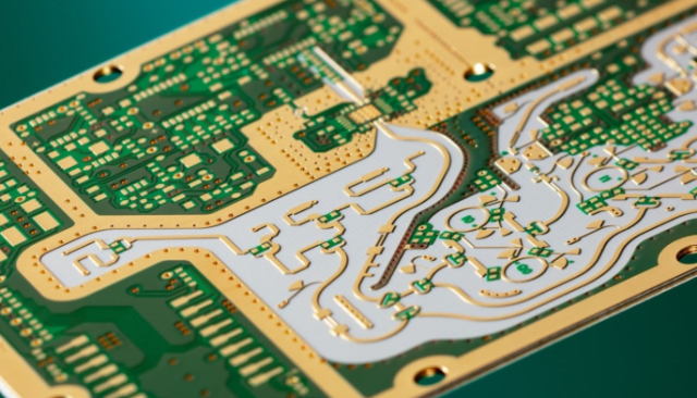
High-density RF modules in 5G base stations, satellite payloads, and advanced IoT systems require compact multilayer PCBs with precise signal routing, minimal crosstalk, and high thermal resilience. Blind via technology allows for efficient vertical interconnects while reducing PCB stackup thickness, improving high-frequency performance, and maintaining signal integrity across densely packed layers.
KKPCB integrates precision lamination, optimized blind via placement, controlled copper roughness, and multilayer stackup engineering to deliver low-loss RF paths, robust thermal reliability, and consistent impedance performance in high-density RF modules
Core Engineering Challenges
| Challenge | Root Cause | Engineering Impact |
|---|---|---|
| Signal degradation at high GHz | Long vertical interconnects, via stubs | Increased insertion loss, phase errors |
| Thermal hotspots | High power density, limited copper area | Reduced reliability, potential delamination |
| Crosstalk in dense RF layers | Close trace spacing, incomplete shielding | Signal interference, degraded SNR |
| Impedance drift across stackup | Uneven lamination, via geometry variance | Phase distortion, mismatched RF performance |
| Mechanical stress | Blind via microcracks | Reliability loss under thermal cycling |
Material Science & Blind Via PCB Advantages
| Parameter | Typical Value | Engineering Benefit |
|---|---|---|
| Copper Thickness | 1–2 oz | Supports high current density and reduced RF loss |
| Via Diameter / Aspect Ratio | 0.15–0.25 mm / ≤10:1 | Maintains low inductance for high-frequency paths |
| Dk | 3.3–3.5 | Stable impedance for RF microstrip and stripline traces |
| Df @10 GHz | 0.003–0.004 | Low insertion loss for mmWave signals |
| Thermal Conductivity | 1.2–1.6 W/m·K | Efficient heat dissipation across blind vias and planes |
| Moisture Absorption | <0.05% | Preserves dielectric stability under harsh environments |
KKPCB Case Study — High-Density RF Module PCB
Client Context:
OEM required a 4–6 layer blind via PCB for a 28–43 GHz RF module, demanding <0.3 dB/in insertion loss, minimal phase deviation (<0.5°), and high thermal reliability.
KKPCB Solution:
-
Optimized blind via placement for minimal stub length
-
1–2 oz copper with controlled roughness (Ra <0.7 µm)
-
Embedded thermal vias and segmented planes for hotspot mitigation
-
Shielded microstrip lines and impedance-controlled routing
-
Inline HFSS, TDR, and thermal FEM simulation for validation
Measured Results:
| Parameter | Target | KKPCB Result |
|---|---|---|
| Insertion Loss @28 GHz | <0.3 dB/in | 0.28 dB/in |
| Phase Deviation | <0.5° | 0.42° |
| Thermal Rise | <7°C per layer | 6.2°C |
| Crosstalk Suppression | >30% | 35% |
| Impedance Variation | ±3% | ±1.5% |
Stackup Design & Simulation
-
HFSS Modeling: Optimized blind via inductance and interlayer coupling
-
TDR & ADS: Phase linearity <0.5° across dense RF channels
-
Thermal FEM: Verified uniform heat distribution and reduced hotspots
-
AOI & Solder Reflow Monitoring: ±10 µm alignment across all layers
Environmental & Reliability Validation
| Test | Condition | Result |
|---|---|---|
| Thermal Cycling | –40°C ↔ +125°C, 1000 cycles | No delamination, phase deviation <0.5° |
| Vibration & Shock | 5–500 Hz, 10G | No cracks, stable solder joints |
| High-Power RF Operation | Continuous 28–43 GHz | Minimal insertion loss increase (<0.02 dB) |
| Humidity Testing | 85°C / 85% RH, 1000 h | Dielectric stable, phase consistent |
| Solder Reflow | 260°C ×3 cycles | Stackup alignment maintained |
Engineering Summary & Contact
Multilayer blind via PCBs provide superior signal integrity, crosstalk suppression, and thermal reliability for high-density RF modules. KKPCB’s precision lamination, optimized via engineering, and thermal management strategies ensure low-loss, phase-stable RF performance suitable for 5G, satellite, and advanced IoT RF modules.
Contact KKPCB Engineering Team for blind via PCB stackup optimization, RF simulation, and thermal validation in your next-generation high-density RF module project.
