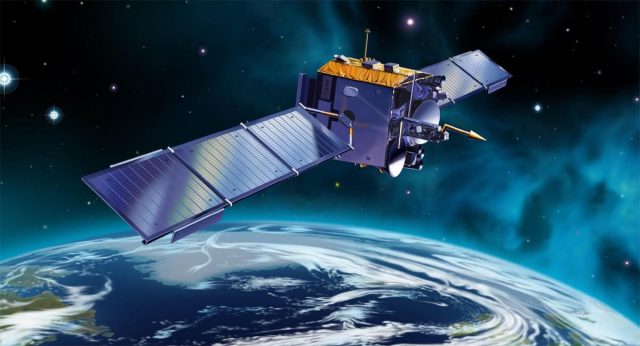
The shift toward high-throughput satellites, beam-steerable phased arrays, and broadband constellations has transformed how engineers design the satellite PCB at the core of every RF payload. In orbit, a PCB cannot rely on airflow, enclosure shielding, or serviceability. The board must deliver low-loss RF routing, stable dielectric behavior, and consistent electrical performance throughout years of exposure to vacuum, cosmic radiation, atomic oxygen, and extreme thermal cycling.
For this reason, low-loss satellite PCB architectures are now central to the design of spaceborne RF payloads. They support high-frequency communication links across L-, S-, X-, Ku-, Ka-, and even Q/V-band channels where material purity and routing precision directly determine link efficiency, gain calibration, and phase coherence.
Low-Loss PCB Materials: The Foundation of Spaceborne RF Performance
The dielectric and conductor losses tolerated in terrestrial RF systems become unacceptable in space. Satellite payloads require PCB materials engineered for:
• Extremely low Df (dissipation factor)
• Stable Dk (dielectric constant) over temperature swings
• Radiation resistance and minimal aging
• Low moisture absorption
• Predictable RF behavior beyond 20–40 GHz
Common materials used in satellite PCB architectures include:
• Rogers RO3003, RO4350B, RO4835
• Ceramic-filled PTFE laminates
• Low-profile copper foils for reduced conductor loss
• Hybrid multilayer stackups combining PTFE + hydrocarbon composites
These materials maintain signal strength, phase linearity, and low insertion loss even when the payload is exposed to ±150°C thermal cycles or deep-space vacuum outgassing.
Architectural Engineering for Low-Loss RF Routing
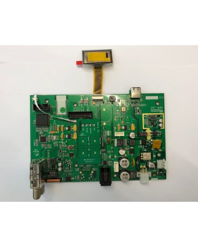
In a spaceborne RF payload, the PCB becomes part of the RF chain, interfacing transceiver ICs, filters, LNAs, PAs, couplers, and waveguide transitions. To preserve signal integrity, boards must incorporate:
• Microstrip or GCPW (grounded coplanar waveguide) RF traces
• Ultra-tight impedance control (±5% or better)
• Back-drilled or blind vias to suppress resonant stubs
• Smooth copper surfaces to reduce conductor attenuation
• Controlled dielectric thickness for predictable propagation delay
These routing strategies ensure stable RF gain, minimal phase distortion, and clean S-parameters across the operating band.
EMI Immunity and Isolation in Satellite RF PCB Designs
With multiple RF, digital, and power domains compressed into compact payload modules, EMI suppression becomes essential. Satellite PCBs rely on:
• Via fences around RF transmission lines
• Segregated RF zones with isolated return paths
• Multilayer stackups with continuous ground reference planes
• Shielding walls and cavity structures
• Filtering and power integrity conditioning
A well-engineered satellite PCB prevents coupling between high-power amplifiers and sensitive low-noise receivers, preserving the system noise figure and link budget.
Thermal Stability in Vacuum Environments
Satellite electronics lack convective cooling, so PCBs must dissipate heat through conduction alone. Low-loss PCB stacks integrate:
• Heavy copper planes for thermal spreading
• Metal-backed substrates
• Ceramic-based laminates with high thermal conductivity
• Controlled CTE (coefficient of thermal expansion) to avoid mechanical stress
This enables stable RF performance across extreme temperature swings, ensuring long-term reliability in orbit.
Reliability Engineering for Spaceborne Qualification
Space-grade satellite PCBs must survive:
• Thermal vacuum cycling
• Vibration and shock loads during launch
• Radiation exposure (TID and SEE)
• Outgassing requirements (NASA/ESA standards)
KKPCB engineers every satellite PCB with manufacturing precision, material verification, and stackup simulation to ensure the board meets aerospace qualification standards for long-duration missions.
KKPCB’s Expertise in Spaceborne RF PCB Manufacturing
KKPCB provides tailored PCB solutions for satellite communication systems, including:
• Low-loss multilayer RF stackups (4–30 layers)
• Rogers, PTFE, and ceramic-based laminates
• Ultra-stable impedance control
• High-frequency routing for 20–60 GHz payloads
• Advanced via structures (blind, filled, back-drilled)
• Tight material tolerance control for RF predictability
Our approach ensures consistent RF payload performance from prototype to flight models.
Powering the Next Generation of Satellite Communications
As satellite networks move toward higher frequencies and denser payload architectures, the performance of the low-loss satellite PCB becomes central to mission success. With engineered materials, precise routing, EMI isolation, and thermal reliability, KKPCB provides the RF stability required for the next generation of spaceborne communication platforms.
