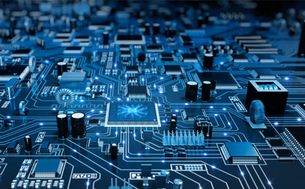
As semiconductor devices become faster, denser, and more complex, chip-level testing has become essential to ensure IC quality, yield, and reliability. Chip Test PCBs serve as the critical interface between the device under test (DUT) and automated test equipment (ATE), providing high-density signal routing, controlled impedance, and precise mechanical alignment for accurate chip validation.
With high-quality chip test PCBs, engineers can efficiently perform functional tests, parametric measurements, and burn-in validation, reducing errors and accelerating time-to-market.
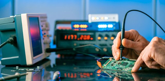
What Is a Chip Test PCB?
A Chip Test PCB is a specialized printed circuit board designed to interface directly with semiconductor chips via probe cards, test sockets, or load boards. Its main functions include:
-
Routing high-density signals from the chip pads to testing equipment
-
Maintaining controlled impedance for high-speed and RF signals
-
Supporting fine-pitch, high-pin-count IC packages
-
Providing mechanical stability for accurate probe alignment and repeated testing
These PCBs are engineered for precision, repeatability, and reliability in demanding semiconductor test environments.
Key Features of Chip Test PCBs
-
High-Density Routing
Supports ICs with thousands of pins, fine-pitch BGAs, and advanced wafer-level packages. -
Controlled Impedance
Ensures signal integrity for high-speed digital and RF testing, preventing reflections and crosstalk. -
Multilayer Stackup Design
Provides dedicated power and ground planes to reduce noise and optimize signal performance. -
Mechanical Precision
Accurate alignment for probe cards and sockets minimizes pad damage and maintains repeatability. -
Thermal and Electrical Reliability
Designed to withstand burn-in testing, high-current measurements, and repeated mechanical stress.
Materials and Stackup Considerations
Choosing the right materials and stackup is critical for performance:
-
High-Tg FR-4 – Suitable for standard IC testing
-
Low-Loss Laminates – For high-speed and RF chip testing
-
Hybrid Stackups – Combine FR-4 and low-loss cores for optimal electrical performance
-
Thermally Stable Materials – Maintain dimensional stability during prolonged testing
Proper material selection ensures signal integrity, mechanical reliability, and consistent test results.
Applications of Chip Test PCBs
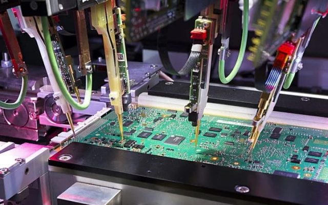
Chip test PCBs are used extensively in:
-
Functional and parametric testing of ICs
-
Wafer-level burn-in and reliability testing
-
Load boards and probe card interfaces in ATE systems
-
Prototype and small-batch chip testing before mass production
-
High-speed digital, RF, and mixed-signal IC validation
These applications rely on the accuracy, repeatability, and high-density routing provided by chip test PCBs.
Choosing a Chip Test PCB Manufacturer
Selecting the right manufacturer is crucial for ensuring test accuracy and reliability. Consider suppliers with:
-
Experience in high pin count, multilayer, and high-speed PCB design
-
Capability for controlled impedance and low-loss routing
-
Support for prototyping, small-batch, and volume production
-
Strong quality control and electrical testing
-
Responsive engineering support for design iteration and optimization
A professional partner ensures repeatable results, high reliability, and fast turnaround.
Conclusion
Chip Test PCBs are vital for modern IC validation, providing high-density routing, controlled impedance, and mechanical precision. Partnering with an experienced manufacturer ensures accurate IC testing, reliable burn-in validation, and seamless integration with ATE systems, enabling faster development cycles and higher-quality semiconductor products.
