Performance required for ceramic substrates and packages
Ceramic substrates and IC packages are used for semiconductor packages and electronic modules, of which the speedy operation and high integration are advancing, and sensor modules, of which the high precision and high sensitivity is advancing.
The performance required for these applications is as follows.
- Dimensional stability and flatness
- Supports various mounting forms (wire bonding, flip chip bonding, SMT, etc.)
- The coefficient of linear expansion is close to that of silicon
- Small size with fine wiring
- Frequency characteristic
- High reliability including heat resistance and humidity resistance
Listed below are KOA’s LTCC boards that satisfy the above conditions.
Applications of LTCC substrates
- Microwave and millimeter-wave substrate for high frequency module
- Interposer for semiconductor packages
- Sensor module package such as MEMS
- High reliability module for aerospace and industrial applications
Click here for the product information on LTCC substrate
Features of KLC series (LTCC substrate)
- Low dielectric loss characteristics (tan δ) and low resistance conductor with small electrical loss, which is suitable for high frequency applications
- Less variation in size and characteristics of each production lot and within each lot due to our unique manufacturing technology
- High-density wiring realized by improved stacking alignment accuracy
- Accurate control of substrate thickness and cavity shape
- Built-in resistor, inductor, and capacitor functions in the substrate and package
High frequency applications
LTCC substrates is a type of ceramic multilayer substrate. It is fired at a lower temperature than a high-temperature fired ceramic substrate (HTCC substrate) whose main component is alumina, and Ag. And it uses Ag, which has the low conductor resistance, as a inner layer conductor. Followings are the electrical characteristics it has.
- Low dielectric loss (tan δ)
- Low conductor resistance )
Low dielectric loss and low conductor resistance lead to low electrical loss at the high frequencies. Having lower dielectric loss than resin substrates, and the conductor with better electrical conduction than that of HTCC substrates, it is generally the most suitable choice for the high-frequency applications.
KKPCB develops and provides a wide variety of ceramics for package applications. Material properties of typical multilayer ceramics are as follows:
| CERAMIC MATERIAL OPTIONS |
ELECTRICAL | THERMAL | MECHANICAL | CONDUCTOR MATERIAL | ||||||
|---|---|---|---|---|---|---|---|---|---|---|
| Dielectric Constant | Dielectric Loss Angle (x1.0E-4) |
CTE(ppm/K) (RT-400°C) |
Thermal Conductivity (W/mK) |
Flexural Strength (MPa) |
Young’s Modulus of Elasticity (GPa) |
|||||
| 1MHz | 2GHz | 1MHz | 2GHz | |||||||
| Alumina (Al2O3) |
A473 | 9.1 | 8.5 | 5 | 10 | 6.9 | 18 | 400 | 270 | W, Mo |
| A440 | 9.8 | _ | 24 | _ | 7.1 | 14 | 400 | 310 | W, Mo | |
| A443 | 9.6 | _ | 5 | _ | 6.9 | 18 | 460 | 310 | W, Mo | |
| AO610W | 9.2 | 9.0 | 9 | 11 | 6.9 | 17 | 460 | 281 | CuW | |
| AO630 | 9.3 | 9.1 | 5 | 23 | 7.0 | 16 | 460 | 275 | CuW | |
| AO700 | 9.4 | 9.2 | 6 | 6 | 7.2 | 21 | 620 | 315 | Mo | |
| AO800 | 9.4 | 9.4 | 4 | 13 | 7.5 | 16 | 740 | 300 | CuW, Mo | |
| AlN | AN242 | 8.7 | 8.6 | 1 | 170 | 4.7 | 150 | 400 | 320 | W |
| LTCC | GL570 | 5.6 | 5.7 | 3 | 7 | 3.4 | 2.8 | 200 | 128 | Cu |
| GL580 | 6.2 | 6.1 | 4 | 16 | 10.4 | 2.0 | 270 | 103 | Cu | |
| GL771 | 5.3 | 5.2 | 8 | 36 | 12.3 | 2.0 | 170 | 74 | Cu | |
| GL773 | 5.7 | 5.8 | 5 | 23 | 11.7 | 1.9 | 280 | 95 | Cu | |
- Material characteristics mentioned above are typical values.
These values may change upon further improvement or modification of these materials and processes.
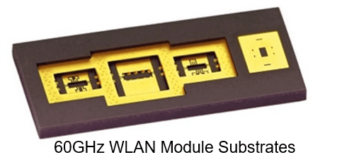
Millimeter-wave module
At high frequencies such as millimeter wave, the LTCC substrate has the advantage over the fluororesin substrate in the easiness of multilayering.
It also provides the following benefits:
- Since the coefficient of thermal expansion is close to that of silicon, the Si-based semiconductor bare chip can be mounted easily.
- High heat dissipation due to higher thermal conductivity by one digit compared with fluororesin substrate
- High moisture resistance due to its non-water-absorbing characteristic
- High-precision cavity formation enables downsizing
Above characteristics show that the LTCC substrates are suitable for semiconductor mounting, modules and packages for millimeter-wave band.
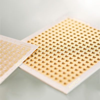
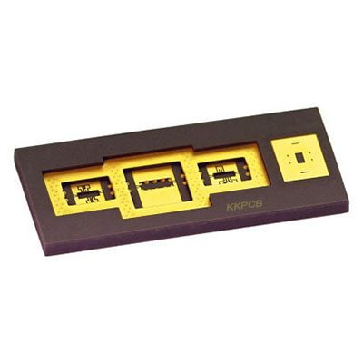
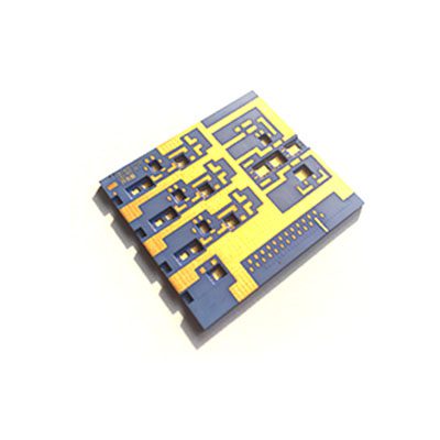
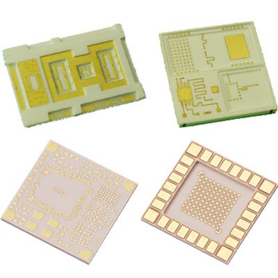
Cavity formation for packages
 Cavity refers to the hollow space formed on a substrate, where semiconductor, sensor and other components are mounted. It enables the downsizing of module and the improvement of its characteristics.
The high dimensional accuracy of cavity and the forming of complex cavity shapes are available on KOA’s LTCC. Also, the positioning accuracy of the pads for component mounting is high, making it suitable for flip-chip mounting.
It also supports complex cavity shapes for multi-chip packages.
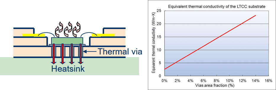
Improvement of the heat dissipation by thermal via
For semiconductor chips that generate a large amount of heat, thermal conductivity and heat dissipation can be improved by forming a thermal via directly under them.
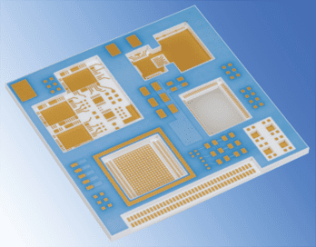
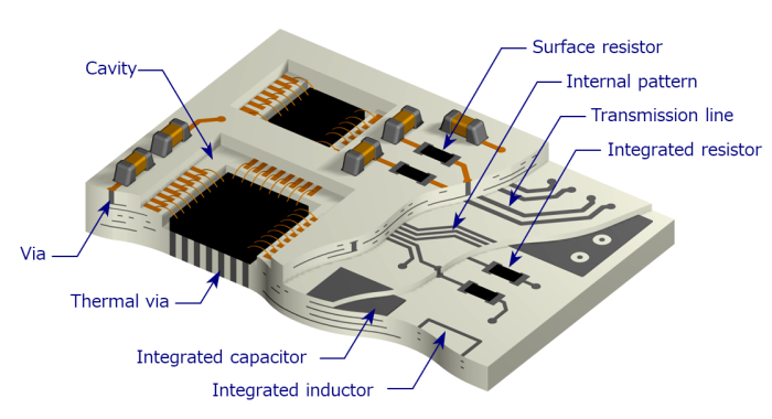
Structure of LTCC substrate
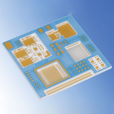
The figure below is an example of a module using the LTCC substrate.
Inner layer wiring is formed on each layer and the layers are connected by via holes. Inductors, capacitors and strip lines for high frequencies can be formed in the LTCC substrate with a ceramic multilayer structure.
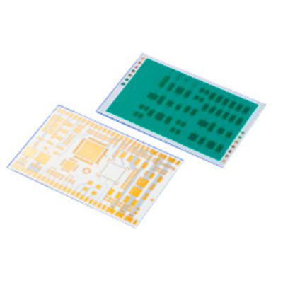
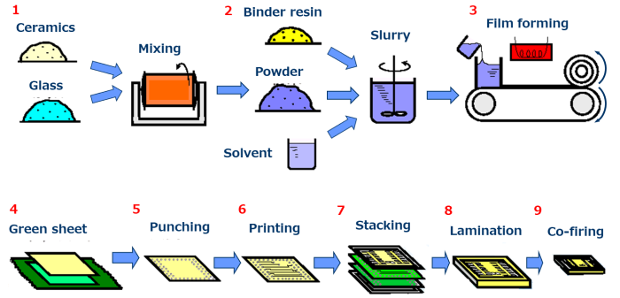
Manufacturing process
- Ceramics and glass powder are mixed.
- An organic binder and solvent are added to the mixed raw materials and dispersed until they become uniform. It makes a material called slurry, which is the basis of a green sheet.
- Slurry is spead on the PET film and dried in the oven to roll-up. This sheet raw ceramics is called “green sheet”
- Green sheet is cut-out to the square shape.
- Through holes are created to make via holes for electrical conductivity.
- Via holes are filled and circuit pattern is printed on the green sheet.
- Several layers are prepared and stacked to make multilayer circuit.
- Sheet block is laminated and fired to make LTCC multilayer substrate.
- Surface of the substrate is plated, and then substrate is separated into pieces depending on requirements.
Manufacturing Process:
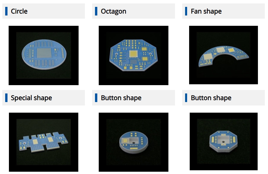
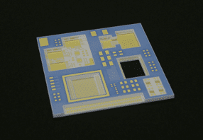
Custom shape package (example)