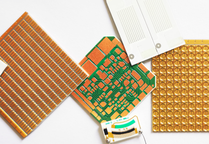
A Ceramic PCB is a substrate technology selected when thermal limits, electrical insulation, and mechanical stability become primary system constraints. In high-power and high-voltage electronic systems, ceramic substrates are not simply alternatives to organic laminates—they function as integrated thermal and structural elements within the overall design architecture.
Ceramic PCB as a Thermal Path Element
In power electronics, heat must be removed efficiently at the source. Unlike FR-4 or metal-core PCBs that rely on secondary heat-spreading mechanisms, a Ceramic PCB provides a direct, low-resistance thermal path from semiconductor devices to the heat sink.
Ceramic substrates enable:
-
Rapid vertical heat transfer away from active devices
-
Uniform thermal distribution across the substrate
-
Reduced thermal gradients that induce mechanical stress
This makes Ceramic PCB technology especially effective in IGBT, MOSFET, SiC, and GaN power modules.
Electrical Insulation and High-Voltage Capability
Ceramic PCB materials inherently offer high dielectric strength, allowing designers to achieve reliable electrical isolation even at elevated voltages. This characteristic supports compact layouts without compromising safety or reliability.
From an engineering standpoint, Ceramic PCB enables:
-
High breakdown voltage with thin dielectric layers
-
Stable electrical insulation across temperature extremes
-
Reduced risk of partial discharge or insulation degradation
These properties are essential in high-voltage converters, inverters, and industrial power systems.
Mechanical Stability and Reliability
Ceramic PCBs exhibit excellent dimensional stability due to their inorganic structure. Unlike organic laminates, ceramics do not soften at elevated temperatures, maintaining rigidity under continuous thermal stress.
Mechanical advantages include:
-
Minimal warpage under high-temperature operation
-
High resistance to thermal cycling fatigue
-
Stable via and metallization interfaces
This stability contributes directly to long-term reliability in harsh operating environments.
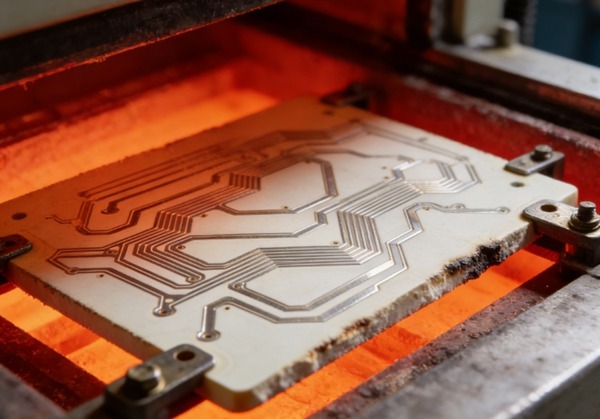
Ceramic PCB Manufacturing Technologies
Several manufacturing approaches are used depending on application requirements:
-
Direct Bonded Copper (DBC) for high-current and power modules
-
Active Metal Brazing (AMB) for improved mechanical robustness
-
Thick-film and thin-film ceramic processes for precision circuits
Each technology offers different trade-offs between thermal performance, mechanical strength, and manufacturing complexity.
Application Domains
Ceramic PCBs are widely adopted in systems where power density and reliability outweigh cost considerations, including:
-
Power conversion and motor drive modules
-
EV and charging infrastructure
-
Aerospace and defense electronics
-
High-power LED and laser systems
-
Industrial automation and renewable energy systems
Engineering Perspective
A Ceramic PCB is best understood as an enabler of thermal and electrical integrity rather than a conventional PCB substrate. By integrating heat dissipation, electrical insulation, and mechanical stability into a single platform, ceramic substrates allow engineers to push power density limits while maintaining system reliability.
KKPCB supports Ceramic PCB solutions through material selection guidance, DBC/AMB process control, and power-oriented layout engineering, helping customers achieve predictable thermal and electrical performance.
