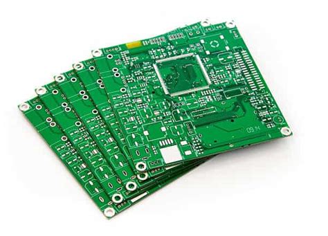
A Mixed Signal IC Test PCB is a critical semiconductor test PCB designed to validate integrated circuits that combine analog and digital functions on a single chip. These ICs are widely used in power management, sensor interfaces, data converters, communication systems, and automotive electronics. Due to the coexistence of sensitive analog signals and high-speed digital signals, mixed signal IC testing requires carefully engineered PCB layouts to ensure accuracy, stability, and repeatability during Automated Test Equipment (ATE) validation.
As mixed signal ICs continue to increase in integration density and operating frequency, the design and manufacturing quality of the test PCB directly affects measurement precision, noise performance, and overall test yield.
Key Design Challenges in Mixed Signal IC Test PCBs

1. Analog and Digital Signal Isolation
Mixed signal IC test PCBs must effectively isolate low-level analog signals from high-speed digital switching noise. Proper partitioning, ground separation, and return path control are essential to minimize crosstalk and signal coupling.
2. Controlled Impedance and Signal Integrity
High-speed digital interfaces and clock signals require precise controlled impedance, trace length matching, and impedance consistency to ensure reliable test results and prevent measurement errors.
3. Low-Noise Power Distribution Network (PDN)
A well-designed power and ground structure with optimized decoupling ensures stable voltage levels and suppresses noise, which is especially critical for sensitive analog circuits such as ADCs and DACs.
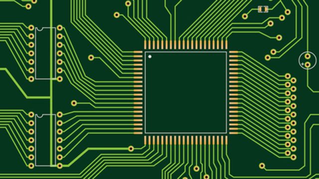
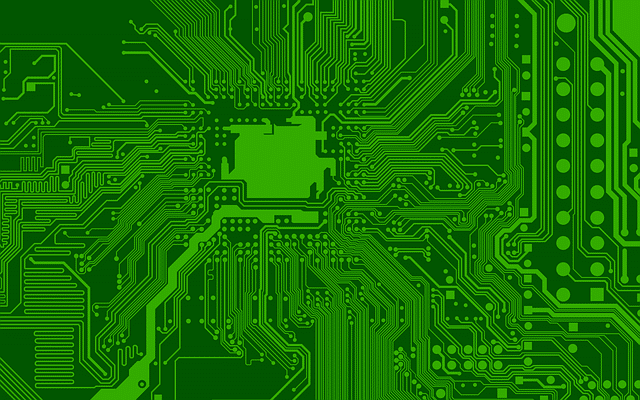
4. High Pin Count and Fine-Pitch Routing
Modern mixed signal ICs often feature high pin count packages and fine-pitch interfaces, demanding HDI PCB technology, microvias, and multilayer stackups for reliable signal access and routing.
5. Thermal and Mechanical Stability
Stable mechanical structure and material selection help maintain dimensional accuracy and electrical performance during repeated test cycles and temperature variations.
Typical Applications of Mixed Signal IC Test PCBs
Mixed signal IC test PCBs are widely used in:
-
Analog-to-Digital Converter (ADC) and Digital-to-Analog Converter (DAC) testing
-
Power management IC (PMIC) validation
-
Sensor interface and signal conditioning IC testing
-
Automotive mixed signal IC qualification
-
Communication and industrial control IC testing
These applications demand high measurement accuracy, repeatability, and low noise performance.
Manufacturing Requirements for Mixed Signal IC Test PCBs
Producing high-quality Mixed Signal IC Test PCBs requires advanced manufacturing capabilities, including:
-
Multilayer and HDI PCB fabrication
-
Fine-line etching and microvia processing
-
Controlled impedance verification and testing
-
High pin count PCB manufacturing
-
Strict electrical and dimensional tolerance control
-
Support for prototype, small batch, and volume production
Precise manufacturing ensures consistent performance across multiple test boards and test cycles.
Why Mixed Signal IC Test PCB Quality Matters
Poorly designed or manufactured mixed signal test PCBs can lead to:
-
Increased noise and unstable measurements
-
Signal interference between analog and digital domains
-
Inconsistent test results and reduced yield
-
Longer debug and validation cycles
A professionally engineered Mixed Signal IC Test PCB ensures accurate, repeatable testing, improves test efficiency, and reduces overall development and production costs.
Conclusion
The Mixed Signal IC Test PCB plays a vital role in validating today’s highly integrated ICs that combine analog precision with digital speed. With optimized layout techniques, controlled impedance, low-noise power design, and high-density routing, these test boards provide reliable and repeatable performance in demanding ATE environments.
Choosing an experienced semiconductor test PCB manufacturer ensures high-quality mixed signal test solutions that support faster validation, higher yield, and long-term product reliability.
