What Is a Burn-in PCB?
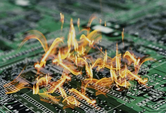
A Burn-in PCB is a specialized printed circuit board designed for stress testing and reliability verification of electronic components and assemblies. During burn-in testing, components are subjected to elevated temperatures, voltage, or current to identify early-life failures and ensure long-term reliability.
Unlike standard PCBs, Burn-in PCBs must withstand high thermal stress, high current density, and repeated cycles without performance degradation, making material selection and design crucial.
Key Design Requirements for Burn-in PCB
Designing an effective Burn-in PCB requires careful attention to several factors:
-
Thermal management
Copper planes, thick copper layers, and metal-core substrates help dissipate heat efficiently. -
High-current handling capability
Traces and vias must support the required current during testing without overheating. -
Mechanical durability
Boards must endure repeated insertion into burn-in fixtures. -
Stable electrical performance
Minimal impedance variations under high temperature and current conditions. -
Test point accessibility
Ensures easy connection to test equipment and monitoring systems.
Proper design ensures that Burn-in PCBs deliver consistent stress testing results.
Materials Used in Burn-in PCB
Burn-in PCBs often require specialized materials to handle high thermal and electrical stress:
-
FR-4 high-temperature laminates
Suitable for moderate burn-in conditions. -
Metal-core PCBs (MCPCB)
Excellent for heat dissipation in high-power applications. -
Ceramic PCBs
High thermal stability and low expansion for precision testing. -
High-reliability laminates
Ensures performance over repeated thermal cycles.
Material choice directly impacts board reliability and test accuracy.
Burn-in PCB Manufacturing Considerations
Burn-in PCB manufacturing requires strict quality and process control:
-
Thick copper plating and robust vias
To handle high current and thermal stress. -
Precise layer alignment and lamination
Prevents warpage under repeated thermal cycles. -
High-quality surface finish
ENIG, hard gold, or immersion silver for reliable connections. -
Electrical and thermal testing
Ensures boards meet burn-in requirements before shipment.
Experienced manufacturers ensure Burn-in PCBs maintain performance throughout testing.
Advantages of Burn-in PCB
Using a Burn-in PCB provides multiple benefits:
-
Detect early-life failures in components before mass production.
-
Verify product reliability under stress conditions.
-
Reduce warranty costs by ensuring only robust products are shipped.
-
Provide repeatable and controlled test conditions for high-volume electronics.
Burn-in PCBs are an essential part of quality assurance in electronics manufacturing.
Applications of Burn-in PCB
Burn-in PCBs are widely used in industries requiring high reliability:
-
Semiconductor burn-in testing
For ICs, microcontrollers, and memory devices. -
LED and display modules
Thermal cycling to verify longevity. -
Power electronics and automotive modules
High-current stress testing. -
Medical electronics
Ensures device reliability under continuous operation. -
Telecommunication and networking equipment
Detects early failures in mission-critical systems.
Burn-in PCBs ensure products meet strict reliability and performance standards.
Conclusion
A Burn-in PCB is a specialized tool for performing accelerated stress testing to ensure the reliability and durability of electronic components and assemblies. From thermal management and high-current design to robust materials and precise manufacturing, every aspect is critical to achieving consistent results.
Partnering with an experienced Burn-in PCB manufacturer ensures high-quality boards capable of withstanding demanding test conditions, reducing failures, and enhancing product reliability.
