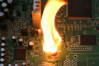
A Burn-in Board PCB is a specialized semiconductor test PCB used during the burn-in process, where integrated circuits are operated under elevated temperature, voltage, and extended time conditions to detect early-life failures. This testing stage is critical for improving IC reliability before devices enter mass production or high-reliability applications.
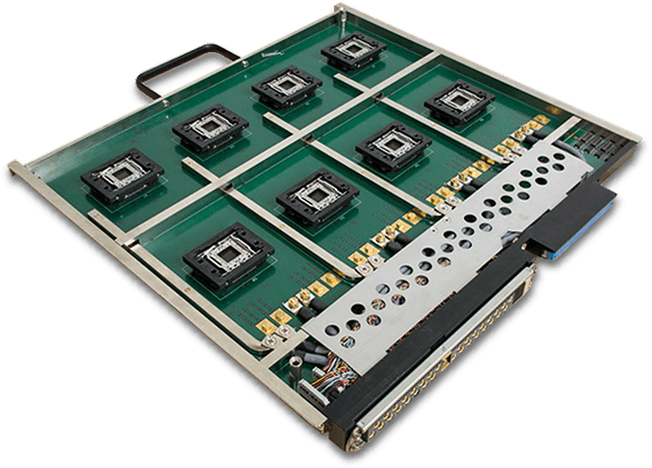
Burn-in boards serve as the electrical and mechanical interface between packaged ICs and Automated Test Equipment (ATE), maintaining stable signal transmission and power delivery throughout prolonged stress testing cycles.
Why Burn-in Testing Requires Specialized PCBs
Unlike functional or parametric testing, burn-in testing focuses on long-duration stability rather than short measurement cycles. A Burn-in Board PCB must therefore withstand:
-
Extended high-temperature operation
-
Repeated thermal cycling
-
High current and voltage stress
-
Long continuous test durations
Any PCB instability can directly affect test accuracy, yield, and overall reliability evaluation.
Key Design Characteristics of Burn-in Board PCBs
1. High Pin Count and Dense Interconnects
Burn-in boards often support ICs with hundreds or thousands of pins, requiring HDI routing, fine-line traces, microvias, and multilayer stackups to ensure reliable electrical connections.
2. Thermal Stability and Material Selection
Burn-in environments demand PCB materials with high Tg, low CTE, and excellent thermal endurance, ensuring dimensional stability and consistent electrical performance during prolonged heating.
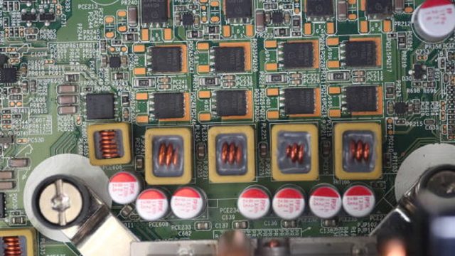
3. Robust Power Distribution Network (PDN)
Stable power delivery is essential during burn-in. Optimized power and ground planes, low-impedance routing, and decoupling strategies prevent voltage drops and reduce electrical stress artifacts.
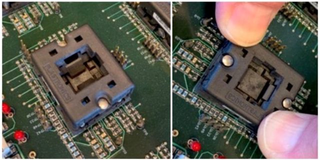
4. Mechanical Precision and Flatness Control
Burn-in boards must maintain excellent flatness and mechanical alignment to ensure reliable socket or fixture contact throughout long test cycles.
5. Reliability-Oriented Design
Thicker copper, reinforced vias, and conservative design rules help prevent electromigration, via fatigue, and trace degradation during extended operation.
Typical Applications of Burn-in Board PCBs
Burn-in Board PCBs are widely used in:
-
Memory IC burn-in testing
-
Processor and logic IC stress validation
-
Automotive-grade IC reliability screening
-
Industrial and high-reliability semiconductor qualification
-
Power management and mixed-signal IC burn-in
These applications require consistent electrical performance over long periods, often under harsh thermal conditions.
Manufacturing Requirements for Burn-in Board PCBs
Producing reliable burn-in boards requires advanced manufacturing capabilities, including:
-
Multilayer and HDI PCB fabrication
-
High-temperature lamination processes
-
Fine-line etching with tight tolerance control
-
Controlled impedance routing where required
-
Prototype, small batch, and volume burn-in board production
Strict process control ensures that each board delivers repeatable performance across multiple burn-in cycles.
Why Burn-in Board PCB Quality Is Critical
Low-quality burn-in boards can cause:
-
Intermittent electrical contact during long tests
-
False failures or missed early-life defects
-
Reduced burn-in yield and test efficiency
-
Increased downtime and higher operational cost
A high-quality Burn-in Board PCB ensures accurate stress testing, consistent results, and reliable IC screening.
Conclusion
The Burn-in Board PCB is a cornerstone of semiconductor reliability testing, enabling early failure detection through long-duration stress testing. With high pin count support, thermal stability, robust power delivery, and precision manufacturing, burn-in boards provide dependable performance in demanding ATE environments.
Partnering with an experienced burn-in board PCB manufacturer ensures reliable testing solutions that improve IC quality, yield, and long-term product performance.
