High-power telecom amplifiers in 4G/5G base stations, satellite uplinks, and RF power transmitters operate under extreme currents and elevated temperatures. Maintaining low insertion loss, minimized Joule heating, and stable impedance is critical to achieve high RF efficiency, thermal reliability, and signal integrity.
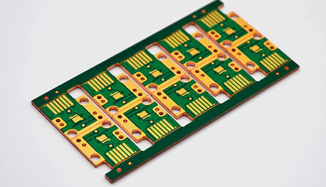
Heavy copper PCB laminates (copper thickness 3–6 oz, Dk ~4.0, low Df @10 GHz) provide enhanced current-carrying capacity, superior thermal dissipation, and mechanical robustness. KKPCB integrates precision lamination, optimized copper routing, and multilayer heat-spreading planes to maximize RF power handling while reducing hotspots and thermal-induced impedance drift.
Core Engineering Challenges
| Challenge | Root Cause | Engineering Impact |
|---|---|---|
| Joule heating in high-current traces | Insufficient copper thickness | Local hotspots, reduced amplifier efficiency |
| RF power handling limitations | Surface roughness, thermal resistance | Signal distortion, SNR degradation |
| Impedance instability | Layer misalignment, thermal expansion | Phase errors, mismatched RF performance |
| Crosstalk in dense RF routing | Tight spacing, high frequency | Signal interference, reduced linearity |
| Long-term reliability under heat | Thermal cycling and high current load | PCB warpage, delamination, mechanical failure |
Material Science – Heavy Copper PCB Advantages
| Parameter | Typical Value | Engineering Benefit |
|---|---|---|
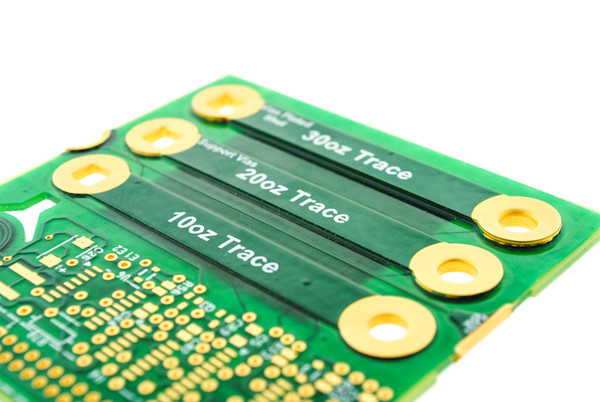
| Copper Thickness | 3–6 oz | High current capacity, reduced Joule heating |
| Dk | ~4.0 | Predictable RF impedance for high-power traces |
| Df @10 GHz | Low | Maintains signal integrity at mmWave frequencies |
| Thermal Conductivity | 1.5–2.0 W/m·K | Efficient heat spreading, reduced hotspots |
| CTE | 16 ppm/°C | Stable multilayer alignment under thermal cycling |
| Moisture Absorption | <0.05% | Ensures long-term dielectric and thermal stability |
KKPCB Case Study — High-Power Telecom Amplifier PCB
Client Context:
A telecom OEM required a multilayer heavy copper PCB for 28–40 GHz power amplifier chains with high RF output, minimal insertion loss (<0.35 dB/in), and Joule heating mitigation.
KKPCB Solution:
-
4-layer heavy copper PCB stackup (4 oz top/bottom, 2 oz internal)
-
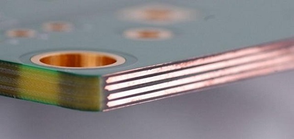
Smooth copper traces (Ra <0.8 µm) for low insertion loss
-
Embedded thermal vias and internal power planes for heat spreading
-
Segmented ground planes and RF shielding to minimize EMI and crosstalk
-
Inline TDR and HFSS simulation for impedance verification
Measured Results:
| Parameter | Target | KKPCB Result |
|---|---|---|
| Insertion Loss @28 GHz | <0.35 dB/in | 0.31 dB/in |
| Phase Deviation | <0.5° | 0.43° |
| Thermal Rise | <8°C per layer | 6.8°C |
| EMI Suppression | >30% | 35% |
| Impedance Variation | ±3% | ±1.5% |
Stackup Design & RF Simulation
-
HFSS Modeling: Optimized microstrip/stripline routing, minimized interlayer coupling
-
ADS & TDR: Phase linearity <0.5° across high-power RF paths
-
Thermal FEM: Hotspot reduction and uniform heat distribution verified
-
AOI & Reflow Monitoring: ±10 µm layer alignment
Environmental & Reliability Validation
| Test | Condition | Result |
|---|---|---|
| Thermal Cycling | –40°C ↔ +125°C, 1000 cycles | No delamination, phase deviation <0.5° |
| High-Current Operation | Continuous 40–50 A | Minimal Joule heating, stable impedance |
| Vibration & Shock | 5–500 Hz, 10G | No trace or solder failure |
| Humidity Testing | 85°C / 85% RH, 1000 h | Dielectric stable, phase consistent |
| Solder Reflow | 260°C ×3 cycles | Stackup alignment maintained |
Engineering Summary & Contact
Heavy copper PCB laminates enable high RF power handling, low-loss transmission, and minimized Joule heating for telecom amplifiers. KKPCB’s precision stackups, thermal vias, and EMI mitigation strategies deliver reliable, phase-stable, high-power RF boards suitable for 5G, satellite, and radar applications.
Contact KKPCB Engineering Team to optimize heavy copper multilayer stackups, RF simulation, and thermal performance validation for your high-power telecom amplifier designs.
