An ATE PCB supplier is a critical technical partner in the development of Automated Test Equipment (ATE) systems used for semiconductor validation, characterization, and production testing. Unlike general-purpose electronics, ATE platforms demand extreme electrical accuracy, mechanical durability, and long-term repeatability, placing significantly higher requirements on PCB design and manufacturing quality.
Technical Demands of ATE PCB Applications
ATE systems operate at the intersection of high-speed digital signaling, precision analog measurement, and repetitive mechanical interaction. As a result, ATE PCBs must support:
-
High-speed test signals with tight controlled impedance tolerance
-
Low-loss transmission paths to minimize attenuation and timing skew
-
Dense interconnect structures for high pin-count devices
-
Mechanical robustness under frequent connector insertion and probing cycles
Any variation in PCB performance directly affects test accuracy, yield analysis, and device qualification, making PCB consistency a system-level requirement rather than a component-level consideration.
Signal Integrity and Impedance Control
One of the primary responsibilities of an ATE PCB supplier is ensuring stable signal integrity across all test channels. This includes:
-
Precise impedance modeling and stackup engineering
-
Consistent dielectric thickness and material control
-
Tight trace geometry tolerance across long routing paths
-
Minimal impedance discontinuity at vias and connectors
High-speed ATE applications often operate in the multi-GHz range, where even minor deviations can introduce measurement error or false test results.
Material Selection for Electrical and Thermal Stability
ATE PCBs commonly require:
-
Low-loss materials to preserve waveform fidelity
-
High TG laminates to maintain mechanical strength under continuous thermal stress
-
Hybrid material stackups for mixed-signal and power-integrated designs
An experienced ATE PCB supplier understands how to balance electrical performance, thermal reliability, and manufacturability without over-engineering the design.
Mechanical Reliability and Structural Integrity
ATE PCBs are subjected to repeated mechanical stress from:
-
Test sockets and high-density connectors
-
Probe card interfaces
-
Long-term fixture mounting and vibration
This requires:
-
Controlled CTE behavior to protect vias and solder joints
-
High peel strength for pad and trace durability
-
Optimized copper distribution to prevent board warpage
Mechanical failure in ATE PCBs often manifests gradually, making upfront structural engineering essential.
Manufacturing Control and Process Consistency
From a manufacturing perspective, an ATE PCB supplier must demonstrate:
-
Stable lamination processes for high layer count boards
-
Accurate drilling and via plating for fine-pitch interconnects
-
Reliable impedance verification and electrical testing
-
Strict process traceability for long product lifecycles
Consistency across builds is critical, as ATE systems frequently require multiple identical boards over extended production periods.
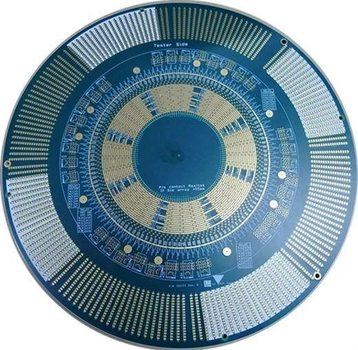
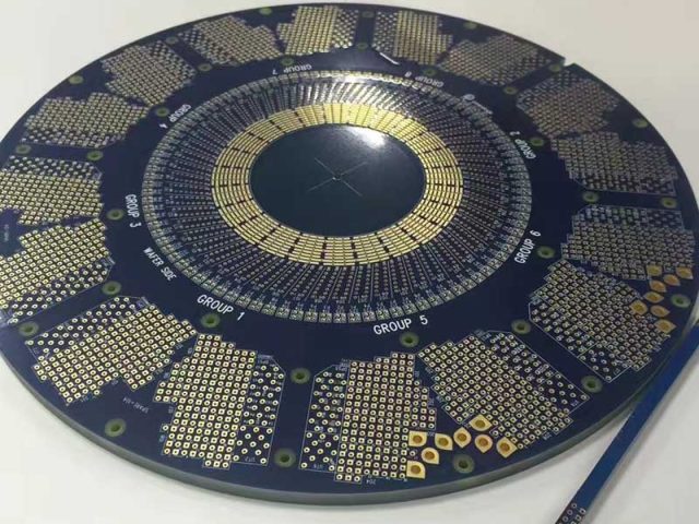
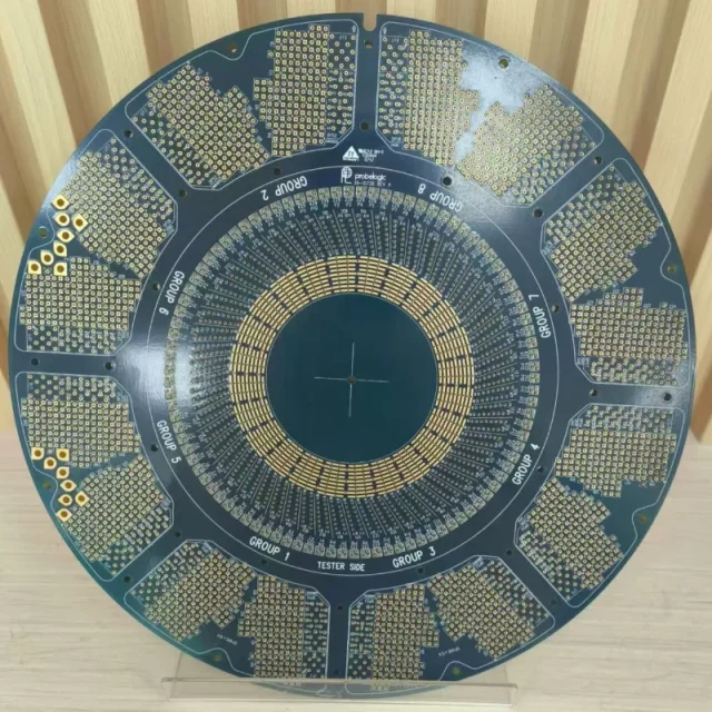
Typical ATE PCB Applications
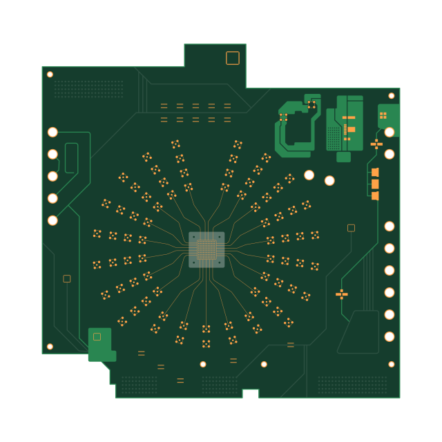
ATE PCBs are widely used in:
-
Semiconductor load boards
-
Probe card assemblies
-
Burn-in and reliability test systems
-
High-speed device characterization platforms
-
Final test and validation equipment
Each application emphasizes precision, durability, and electrical predictability over cost-driven optimization.
Engineering Perspective
Selecting the right ATE PCB supplier is not a procurement decision—it is an engineering risk management decision. A qualified supplier contributes not only fabrication capability, but also material insight, stackup optimization, and process discipline, ensuring the PCB does not become the limiting factor in test system performance.
KKPCB supports ATE PCB projects through controlled impedance manufacturing, advanced material handling, high layer count expertise, and strict quality control, delivering stable performance for demanding automated test environments.
