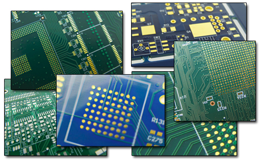
A fast and accurate PCB quotation is critical for electronics designers, hardware engineers, and product managers who are planning prototypes or mass production runs. Providing complete design files and specifications, including Gerber files, Bill of Materials (BOM), PCB layer count, and manufacturing details, allows manufacturers to deliver precise, timely, and optimized PCB pricing.
Without complete information, quotation times can extend, and estimates may include risk buffers, leading to higher costs and longer lead times. This is especially true for high-density multilayer boards, HDI designs, RF/microwave boards, or 5G/IoT applications.

Why Complete Files Accelerate PCB Quotes
| Requirement | Purpose | Benefit |
|---|---|---|
| Gerber Files | Defines copper layers, drills, pads, traces | Ensures accurate fabrication planning |
| BOM (Bill of Materials) | Lists all components, footprints, and suppliers | Allows precise assembly and sourcing cost |
| PCB Layer Count | Specifies signal, power, and ground layers | Influences stackup design, impedance control |
| Manufacturing Requirements | Includes copper weight, dielectric material, tolerances, surface finish | Guarantees correct pricing for specialized materials |
| Controlled Impedance & Trace Width | Critical for RF, high-speed digital, or HDI PCBs | Reduces signal loss and ensures phase fidelity |
| Assembly and Testing Notes | Defines via types, solder mask, and testing steps | Avoids mispricing due to overlooked production steps |
Engineering Considerations
When submitting a PCB for quotation, manufacturers evaluate multiple technical aspects to ensure low insertion loss, reliable signal integrity, and robust thermal performance:
-
Material Selection: FR-4, Rogers, Megtron 7, RO4350B, RO4835, Alumina, or customized high-frequency laminates.
-
Copper Thickness & Surface Roughness: Critical for high-speed digital, RF, and microwave designs.
-
Stackup & Layer Alignment: Impacts impedance accuracy, phase stability, and EMI control.
-
Via Strategy: Through-hole, blind, buried, or stacked microvias affect signal integrity and fabrication complexity.
-
Solder Mask & Surface Finish: ENIG, OSP, or HASL coatings influence assembly yield and long-term reliability.
Providing these specifications upfront allows manufacturers like KKPCB to analyze cost, production complexity, and lead time accurately.
KKPCB Case Study — Prototype to Mass Production
Scenario: A client developing a 6-layer HDI IoT gateway required both prototype and mass production PCB quotes.
Submitted Data:
-
Complete Gerber files for all layers
-
Full BOM with reference designators and manufacturer part numbers
-
Layer count, material type, and copper thickness
-
Assembly requirements including blind vias and controlled impedance traces
KKPCB Results:
-
Delivered a highly accurate quote within 24 hours
-
Suggested design improvements for signal integrity and thermal reliability
-
Optimized both prototype and full production pricing, balancing cost and performance
Outcome: Client proceeded confidently to prototype validation and mass production, ensuring minimal design iteration and predictable costs.
Best Practices for Fast PCB Quotation Requests

-
Provide Complete Gerber Files – Include all copper, drill, solder mask, and silkscreen layers.
-
Submit Detailed BOM – Include component numbers, footprints, and supplier information.
-
Specify Layer Count – Clearly define signal, power, and ground layers.
-
Include Manufacturing Requirements – Material type, copper weight, tolerances, and surface finish.
-
Detail Assembly & Testing Instructions – Via types, solder mask, and post-assembly testing processes.
Following these steps ensures rapid, accurate, and optimized PCB quotations, particularly for high-density, HDI, and RF/microwave PCBs.
Conclusion & Contact
Submitting complete design files and specifications allows KKPCB to provide fast and precise PCB quotations for both prototype and mass production projects. This process ensures reliable cost estimation, optimized manufacturing, and reduced time to market.
Contact KKPCB Engineering Team to submit your Gerber files, BOM, layer count, and manufacturing specifications, and receive a high-density, accurate PCB quotation for your next-generation electronic system.
