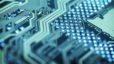
Advanced RF Packaging Requires Hybrid PCB Stackup Technology
As modern RF and microwave systems continue evolving toward:
- 5G and 6G communication
- millimeter-wave radar
- satellite communication
- aerospace RF electronics
- defense microwave systems
- high-density RF modules
- advanced phased-array antennas
the demand for:
- higher integration density
- lower signal loss
- stable impedance control
- compact RF packaging
has increased dramatically.
Traditional PCB stackup structures often struggle to simultaneously achieve:
- high-frequency RF performance
- thermal stability
- multilayer routing density
- mechanical reliability
- cost-effective manufacturing
To solve these challenges, engineers increasingly adopt:
- hybrid PCB stackup design
using: - Duroid 6010 PCB materials
combined with: - FR4 PCB
- low-loss laminates
- multilayer RF PCB structures
A hybrid RF PCB stackup enables:
- optimized RF signal integrity
- improved thermal management
- controlled impedance stability
- high-density microwave routing
- cost-efficient multilayer integration
This article explores:
- hybrid stackup design techniques
- Duroid 6010 PCB characteristics
- multilayer RF PCB engineering
- microwave packaging optimization
- impedance control
- thermal management
- fabrication considerations for high-density RF systems
What Is Duroid 6010 PCB Material?
Overview of Duroid 6010 High-Frequency Laminate
Duroid 6010 PCB material is a high-frequency ceramic-filled PTFE laminate engineered for:
- RF PCB applications
- microwave PCB systems
- millimeter-wave circuits
- aerospace RF electronics
It is widely recognized for:
- high dielectric constant
- low dielectric loss
- stable microwave performance
- excellent thermal reliability
Duroid 6010 is commonly used in:
- compact RF filters
- microwave resonators
- power amplifiers
- antenna systems
- radar modules
Key Characteristics of Duroid 6010 PCB
1. High Dielectric Constant (Dk)
Duroid 6010 typically provides:
- dielectric constant (Dk) ≈ 10.2
Benefits:
- miniaturized RF circuits
- compact microwave structures
- reduced transmission line size
This enables:
- higher RF integration density
- smaller antenna structures
- compact RF packaging
2. Low Dissipation Factor (Df)
Low dielectric loss improves:
- RF transmission efficiency
- insertion loss performance
- microwave signal quality
Applications:
- mmWave PCB
- RF filters
- microwave communication systems
3. Excellent Thermal Stability
Thermal stability improves:
- impedance consistency
- RF measurement reliability
- multilayer PCB durability
This is critical in:
- aerospace electronics
- automotive radar systems
- military RF platforms
4. High-Density RF Integration Capability
The high dielectric constant supports:
- shorter RF wavelengths
- reduced circuit dimensions
- compact microwave layouts
This is ideal for:
- high-density RF packaging
- multilayer RF modules
- miniaturized communication systems
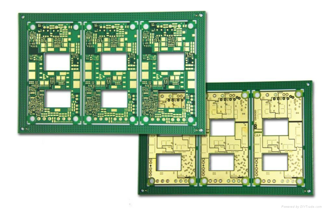
What Is Hybrid PCB Stackup Design?
Definition of Hybrid Stackup PCB Design
A hybrid PCB stackup combines:
- multiple PCB materials
within: - a single multilayer PCB structure
Typical combinations include:
- Duroid 6010 + FR4
- PTFE laminate + low-loss laminate
- RF laminate + high-speed digital PCB material
The goal is to optimize:
- RF performance
- manufacturing cost
- thermal behavior
- routing density
- electrical stability
Advantages of Hybrid Stackup Design Using Duroid 6010 PCB
1. Optimized RF Performance
Duroid 6010 layers provide:
- low-loss RF transmission
- stable impedance control
- excellent microwave signal integrity
This improves:
- insertion loss performance
- RF efficiency
- phase stability
2. High-Density RF Packaging Capability
The high dielectric constant allows:
- reduced RF trace dimensions
- compact microwave routing
- smaller antenna structures
Benefits:
- increased routing density
- miniaturized RF modules
- compact multilayer packaging
3. Cost Optimization
Using Duroid 6010 throughout an entire PCB may increase:
- material cost
- fabrication complexity
Hybrid stackups reduce cost by:
- using RF laminate only in critical RF layers
- using FR4 for digital and power routing
This balances:
- performance
- manufacturability
- overall PCB cost
4. Improved Thermal Management
Hybrid multilayer PCB structures can optimize:
- heat distribution
- thermal conduction
- mechanical stability
Thermal management is critical for:
- RF power amplifiers
- microwave transmitters
- radar systems
5. Enhanced Multilayer Routing Flexibility
Hybrid stackups support:
- RF routing
- digital routing
- power distribution
- grounding optimization
within one integrated PCB platform.
Key Design Considerations for Hybrid Duroid 6010 PCB Stackups
1. Controlled Impedance PCB Design
Controlled impedance is critical for:
- RF transmission lines
- microwave circuits
- high-speed digital interfaces
Important factors:
- dielectric constant
- trace width
- layer thickness
- ground plane spacing
Impedance consistency improves:
- signal integrity
- insertion loss stability
- RF calibration accuracy
2. Microstrip and Stripline Optimization
Hybrid RF PCB designs commonly use:
- microstrip transmission lines
- stripline routing structures
Microstrip advantages:
- easier RF tuning
- lower fabrication complexity
Stripline advantages:
- improved EMI shielding
- better impedance consistency
3. Ground Plane Integrity
Continuous ground planes improve:
- return current stability
- RF shielding
- EMI suppression
- microwave signal quality
Ground via stitching is critical near:
- RF transitions
- antenna feeds
- microwave components
4. Thermal Expansion Matching
Hybrid materials may have different:
- coefficients of thermal expansion (CTE)
Poor CTE matching can cause:
- delamination
- reliability problems
- layer stress
Proper stackup engineering minimizes:
- thermal stress
- mechanical warpage
- multilayer reliability issues
5. Via Structure Optimization
RF vias may introduce:
- parasitic inductance
- impedance discontinuities
- signal reflection
Optimization techniques:
- back drilling
- blind vias
- buried vias
- ground via shielding
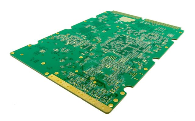
Multilayer RF PCB Stackup Strategies
1. Dedicated RF Signal Layers
Critical RF transmission lines should be placed on:
- low-loss RF laminate layers
This minimizes:
- insertion loss
- dielectric loss
- signal degradation
2. Separate Digital and RF Regions
Isolation between:
- RF circuits
and: - digital circuits
reduces:
- EMI coupling
- switching noise
- RF interference
3. Embedded Ground Planes
Ground planes improve:
- impedance control
- return path stability
- RF shielding
4. Power Integrity Optimization
RF systems require:
- low-noise power distribution
- stable voltage regulation
Decoupling strategies include:
- bypass capacitors
- filtering structures
- isolated power routing
Fabrication Challenges in Hybrid Duroid 6010 PCB Design
1. PTFE Material Processing Complexity
Duroid 6010 requires:
- specialized drilling
- plasma processing
- controlled lamination
2. Multilayer Registration Accuracy
Hybrid stackups require:
- precise layer alignment
- tight dimensional control
Small variations affect:
- impedance consistency
- RF signal quality
3. Copper Roughness Control
At microwave frequencies:
- conductor surface roughness increases RF loss
Low-profile copper foil improves:
- insertion loss performance
- signal integrity
4. Lamination Process Control
Proper lamination ensures:
- stable dielectric thickness
- multilayer reliability
- thermal durability
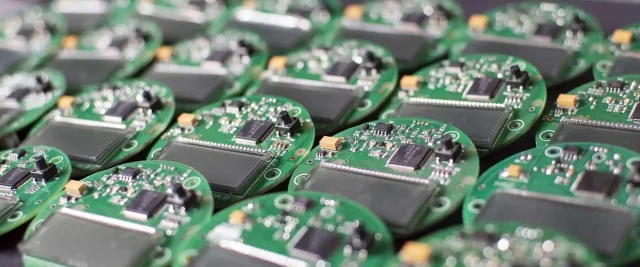
Applications of Hybrid Duroid 6010 PCB Stackups
Hybrid RF PCB stackups are widely used in:
- 5G mmWave communication systems
- phased-array radar
- aerospace RF modules
- satellite communication systems
- microwave backhaul equipment
- RF power amplifiers
- defense communication systems
- automotive radar platforms
Future Trends in Hybrid RF PCB Technology
1. Higher Frequency mmWave Systems
Supporting:
- 77 GHz radar
- 110 GHz communication
- terahertz RF systems
2. Advanced RF Package Integration
Including:
- antenna-in-package (AiP)
- system-in-package (SiP)
- embedded RF modules
3. Ultra-High-Density RF PCB Structures
Future systems require:
- finer RF routing
- thinner laminates
- tighter impedance control
4. AI-Assisted RF PCB Optimization
Using:
- electromagnetic simulation
- automated stackup optimization
- predictive signal integrity analysis
Conclusion
Hybrid stackup design using Duroid 6010 PCB materials provides an advanced solution for:
- high-density RF packaging
- microwave PCB integration
- multilayer RF circuit optimization
By combining:
- Duroid 6010 high-frequency laminate
with: - multilayer PCB engineering
- controlled impedance routing
- optimized grounding
- thermal management strategies
engineers can achieve:
- low-loss RF transmission
- compact microwave layouts
- stable signal integrity
- excellent thermal reliability
- cost-effective RF system integration
As modern RF and microwave technologies continue evolving toward:
- higher frequency
- greater integration
- compact packaging
- ultra-high-speed communication
advanced hybrid RF PCB stackup design will remain essential for next-generation wireless and microwave electronic systems.
