Mastering High-Speed PCB Test Point Design: Precision, Performance, and Signal Integrity
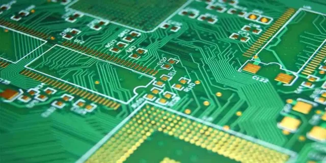
In high-speed printed circuit board (PCB) design, test point placement is far more than a routine step—it’s a science of balance. The miniature metal pads scattered across a PCB may look simple, but their position, size, and electrical behavior can determine whether a product performs flawlessly or fails under load. As circuits evolve toward higher frequencies and faster data transmission, every picosecond and every trace counts.
The Strategic Art of Test Point Placement
High-speed signals behave like living currents of light—sensitive, reactive, and prone to distortion. Test points, if poorly placed, can distort the very signals they’re meant to measure.
Effective placement begins with understanding signal flow. Test points should be positioned where they offer visibility into critical nodes while introducing minimal interference. This often means placing them at trace endpoints or near controlled impedance regions, ensuring signal paths remain unbroken and reflections are minimized.
The enemy here is disruption—crosstalk between traces, electromagnetic interference (EMI), and impedance mismatches. A well-designed test point placement strategy acknowledges these hazards, isolating measurement sites to preserve signal clarity and ensure repeatable test data.
Physical Design: Small Details, Big Impact
A test point’s physical form can quietly alter circuit behavior. The pad diameter, via length, and probe style all contribute parasitic capacitance and inductance. These unwanted electrical echoes distort high-speed signals.
Designers must keep test points compact yet accessible, balancing manufacturability and measurement precision. Using high-impedance probes further reduces loading effects on delicate signals. For extreme-speed applications, surface-mount test points are preferred—they minimize inductance and occupy less real estate than traditional through-hole types.
Ground Reference and Noise Control
Every accurate measurement needs a stable reference. In high-speed PCBs, a solid and continuous ground plane is indispensable. Test points should maintain direct, low-impedance connections to ground to suppress noise pickup and EMI.
Avoid ground splits, route return currents efficiently, and place decoupling capacitors near sensitive test nodes. These measures collectively stabilize voltage levels and improve the reliability of signal analysis.
Accessibility Meets Precision
Engineers must probe hundreds of test points during debugging and validation, often under time pressure. Poorly placed or unlabeled points waste hours. Good test point design considers ergonomics—ensuring access for test probes without mechanical interference from tall components or shielding enclosures.
Each test point should be clearly documented in design files, and ideally grouped logically to streamline automated testing.
Impedance and Thermal Considerations
At gigahertz frequencies, even a minor impedance mismatch can cause reflections that corrupt data integrity. To prevent this, test point geometry and surrounding trace widths should be tuned to maintain consistent impedance. Simulation tools such as HFSS or HyperLynx can model the electromagnetic effects of test pads before production.
Thermal factors also matter. High-speed components can generate localized hotspots, and clustered test points may exacerbate heat concentration. Proper thermal reliefs and spacing maintain both electrical stability and mechanical reliability.
Advanced Approaches: Differential and Automated Testing
Modern high-speed PCBs often employ differential signaling—pairs of traces that carry opposite but complementary signals to minimize noise. Differential test points must therefore be matched precisely, with identical pad geometries and trace lengths to ensure accurate measurement of differential-mode signals without injecting common-mode noise.
The next level of sophistication lies in automation. Integrating test points compatible with Automated Test Equipment (ATE) systems enables rapid, repeatable, and error-free validation. Automated probing not only accelerates the testing process but ensures consistency across production batches.
Material Matters
Material selection is often overlooked but profoundly influences high-frequency behavior. Laminates with low dielectric constants (Dk) and low loss tangents (Df) such as Rogers or Megtron series materials preserve signal fidelity. The PCB stack-up and copper thickness must align with the test point’s intended measurement bandwidth.
Conclusion: Precision as the Foundation of Progress
The placement and design of test points in high-speed PCB layouts reflect a fundamental truth of modern electronics—precision at the microscopic level defines success at the system level.
A test point is more than a pad for measurement; it is a design decision that links engineering foresight to manufacturing reliability. By adhering to principles of controlled impedance, minimal parasitics, stable grounding, and test accessibility, engineers can build PCBs that are not only fast but also verifiably correct.
As technology continues to push into terahertz territories and AI-driven hardware grows more complex, the humble test point remains a silent but indispensable witness to every signal’s journey.
