
In PCB manufacturing and assembly, dimensional stability is a critical factor that directly affects product reliability and production yield.
One common but often underestimated challenge is PCB warpage.
PCB warpage occurs when a circuit board bends, twists, or loses its original flatness due to thermal stress, material characteristics, design imbalance, or manufacturing process variations.
Although warpage may appear as a minor mechanical issue, it can create significant problems during:
- SMT component placement
- Reflow soldering
- Automated assembly
- Electrical testing
- Final product reliability validation
As electronic products become thinner, smaller, and more highly integrated, controlling PCB flatness has become increasingly important for achieving stable production performance.
This article explains the major causes of PCB warpage, its impact on manufacturing, and practical methods to prevent and control deformation.
What Is PCB Warpage?
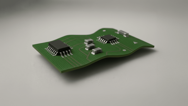
PCB warpage refers to the deformation of a printed circuit board from its designed flat shape.
It mainly appears in two forms:
1. Bow
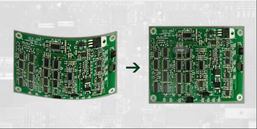
Bow occurs when the PCB bends along one direction, creating a curved surface.
2. Twist
Twist occurs when different areas of the PCB deform unevenly, causing the board corners to no longer remain on the same plane.
Both types of deformation can affect:
- component positioning accuracy
- solder joint quality
- mechanical assembly
- electrical connection reliability
For high-density PCB assemblies, even small deformation can increase manufacturing risks.
Main Causes of PCB Warpage
PCB warpage is usually caused by a combination of material properties, PCB structure, thermal stress, and manufacturing conditions.
1. Thermal Stress During PCB Processing
Thermal stress is one of the most common causes of PCB warpage.
During processes such as:
- lamination
- solder mask curing
- reflow soldering
- thermal testing
the PCB experiences repeated heating and cooling cycles.
Different materials inside the PCB expand and contract at different rates.
For example:
- copper layers
- resin systems
- glass fiber materials
have different coefficients of thermal expansion (CTE).
When thermal expansion is uneven, internal stress accumulates and may cause the PCB to bend or twist.
Reflow Soldering Impact
During SMT assembly, PCBs typically experience temperatures above 200°C during reflow.
If heating or cooling is uneven:
- different PCB areas expand differently
- internal stress increases
- board deformation may occur
This is especially critical for:
- large-size PCBs
- multilayer boards
- high copper density designs
2. Material Selection and PCB Construction
PCB materials have a direct influence on dimensional stability.
Low-Tg Material Risk
Materials with lower glass transition temperatures (Tg) become softer when exposed to high temperatures.
During soldering or thermal cycling, low-Tg materials are more likely to deform.
For applications requiring high reliability, engineers often select:
- High-Tg FR-4
- Low-CTE materials
- High-frequency laminates with stable mechanical properties to improve thermal resistance.
Moisture Absorption
PCB materials can absorb moisture during storage or transportation.
When moisture turns into vapor during soldering, internal expansion pressure may occur.
Possible results include:
- PCB deformation
- delamination
- soldering defects
Proper storage conditions and pre-baking processes help reduce moisture-related risks.
3. PCB Design Imbalance
PCB structure has a significant impact on warpage.
Asymmetrical Layer Stackup
Multilayer PCBs with unbalanced copper distribution may experience uneven stress.
Examples:
- different copper thickness between layers
- uneven plane distribution
- unbalanced dielectric thickness
can create mechanical imbalance during thermal cycling.
Better Design Practices
To reduce warpage risk:
- maintain symmetrical stackup design
- balance copper distribution
- optimize layer arrangement
- avoid excessive copper imbalance
A proper stackup design should consider both electrical performance and mechanical stability.
4. Manufacturing Process Factors
Manufacturing process control also directly affects PCB flatness.
Common manufacturing-related causes include:
Poor Lamination Control
Incorrect:
- temperature profile
- pressure control
- curing conditions
during lamination may create internal stress.
Uneven Heating and Cooling
Rapid or inconsistent cooling can cause different PCB areas to shrink at different rates.
Proper thermal process control helps maintain board stability.
Effects of PCB Warpage
PCB warpage can negatively impact both assembly efficiency and product reliability.
1. SMT Assembly Problems
Modern PCB assembly relies on highly precise automated equipment.
Warped boards may cause:
- inaccurate component placement
- insufficient solder paste contact
- placement errors during pick-and-place
For fine-pitch components such as:
- BGA
- QFN
- CSP
even small deformation may create assembly challenges.
2. Poor Solder Joint Reliability
During reflow soldering, PCB flatness affects solder paste printing and component contact.
Warpage may lead to:
- insufficient solder
- excessive solder
- open circuits
- solder bridging
These defects can reduce long-term product reliability.
3. Electrical and Mechanical Failures
Long-term effects of PCB warpage include:
- cracked solder joints
- damaged vias
- intermittent electrical connections
- reduced product lifespan
For automotive, industrial, and high-reliability electronics, these risks must be controlled before mass production.
How to Prevent PCB Warpage
Preventing PCB warpage requires cooperation between PCB design, material selection, and manufacturing control.
1. Optimize PCB Design
Recommended practices include:
Balanced Stackup Design
Ensure multilayer structures remain symmetrical.
Copper Balance Optimization
Maintain balanced copper distribution across layers.
Proper Board Thickness Selection
Thicker boards generally provide better mechanical stability.
2. Select Suitable PCB Materials
For demanding applications, consider:
Material selection should match:
- operating temperature
- reliability requirements
- assembly process conditions
3. Control Manufacturing Processes
PCB manufacturers should optimize:
Lamination Process
Control:
- temperature
- pressure
- curing time
Reflow Profile
Maintain:
- uniform heating
- controlled cooling rate
- stable temperature distribution
Moisture Management
Implement:
- proper storage
- moisture protection
- pre-baking when required
PCB Warpage Detection Methods
Early detection helps prevent assembly failures.
Visual Inspection
Simple inspection methods can identify:
- visible bending
- uneven corners
- surface deformation
Precision Measurement
Advanced methods include:
- laser measurement systems
- optical inspection
- 3D surface measurement
These tools provide accurate warpage data for quality control.
Production Quality Monitoring
Warpage inspection should be performed after critical stages such as:
- PCB fabrication
- lamination
- reflow soldering
Early detection improves production yield and reduces rework costs.
Can PCB Warpage Be Repaired?
For minor deformation, some correction methods may be possible:
- controlled baking
- mechanical flattening
- thermal stress relief
However, severe warpage may affect internal structures permanently, including:
- copper integrity
- dielectric bonding
- via reliability
Therefore, prevention is always more effective than repair.
Conclusion
PCB warpage is not simply a mechanical issue — it is a manufacturing reliability challenge that affects assembly efficiency, product quality, and long-term performance.
As PCB technologies continue evolving toward:
- higher layer counts
- smaller components
- higher power density
- more demanding applications
controlling PCB deformation becomes increasingly important.
Through optimized:
engineers can reduce warpage risks and improve production consistency.
At KKPCB, our engineering team supports customers with PCB fabrication, PCBA assembly, and DFM analysis to identify potential manufacturing risks before production, helping improve product reliability and mass production readiness.
